Altera Nios Development Board Stratix II Edition User Manual
Page 34
2–24
Reference Manual
Altera Corporation
Nios Development Board Stratix II Edition
May 2007
Board Components
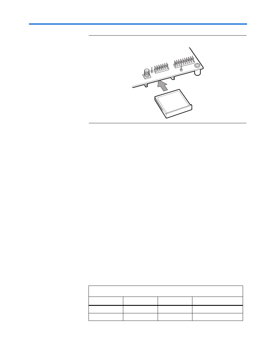
Figure 2–10. CompactFlash Connector
Most pins of CON3 connect to I/O pins on the FPGA. The following pins
have special connections:
■
Pin 13 and 38 of CON3 (VCC) are driven by a power MOSFET that is
controlled by an FPGA I/O pin. These connections allow the FPGA
to control power to the CompactFlash card for the IDE connection
mode.
■
Pin 26 of CON3 (-CD1) is pulled up to 5 V through a 10 k
Ω resistor.
This signal is used to detect the presence of a CompactFlash card;
when the card is not present, the signal is pulled high through the
pull-up resistor.
■
Pin 41 of CON3 (RESET) is pulled up to 5.0 V through a 10 k
Ω
resistor, and is controlled by the EPM7256AE configuration
controller. The FPGA can cause the configuration controller to assert
RESET, but the FPGA does not drive this signal directly.
The CompactFlash connector shares several FPGA I/O pins with
expansion prototype connector PROTO1. Refer to
Connectors (PROTO1 & PROTO2)” on page 2–16
1
Do not connect cards to PROTO1 and CON3 at the same time.
Damage to one or both cards might result.
lists connections between CON3 and the FPGA.
Table 2–13. CompactFlash Pin Table
FPGA Pin
CON3 Pin
Pin Function
Board Net Name
(1)
C1
6
D7
proto1_io0
C2
47
D8
proto1_io1