Altera Nios Development Board Stratix II Edition User Manual
Page 22
2–12
Reference Manual
Altera Corporation
Nios Development Board Stratix II Edition
May 2007
Board Components
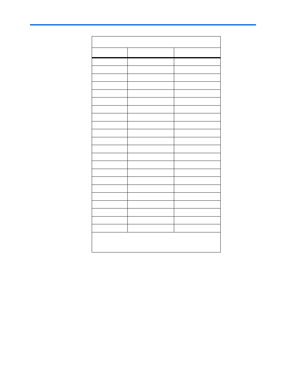
The on-board configuration controller makes assumptions about what
resides where in flash memory. For details refer to
f
See www.amd.com for detailed information about the flash memory
device.
V21
3
fe_a16
W22
54
fe_a17
W21
19
fe_a18
V24
18
fe_a19
V23
11
fe_a20
U24
12
fe_a21
U23
15
fe_a22
R24
2
fe_a23
D15
35
fe_d0
G15
37
fe_d1
E19
39
fe_d2
D20
41
fe_d3
G19
44
fe_d4
D19
46
fe_d5
E20
48
fe_d6
F20
50
fe_d7
H19
32
flash_cs_n
H20
34
flash_oe_n
V26
13
flash_rw_n
H22
16
flash_wp_n
K18
53
flash_byte_n
(1)
W25
17
flash_ry_by_n
Note to
:
(1)
BYTE_n on U5 is pulled low to keep the flash memory in byte
mode which restricts the usable modes of operation.
Table 2–8. Flash Memory Pin Table (Continued)
FPGA Pin
U5 Pin
Board Net Name