Chapter 3 – DFI HU968 User Manual
Page 19
www.dfi .com
Chapter 3 Hardware Installation
19
Chapter 3
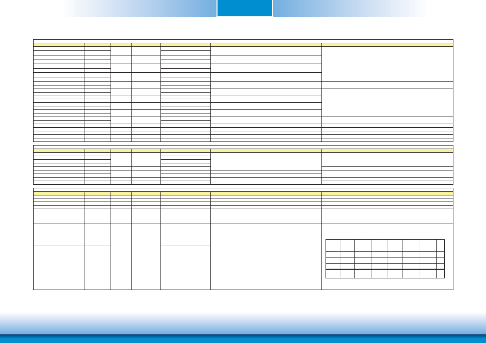
Signal
Pin#
Module Pin Type Pwr Rail /Tolerance
HU968
Carrier Board
Description
LVDS_A0+
A71
LVDS_A0-
A72
LVDS_A1+
A73
LVDS_A1-
A74
LVDS_A2+
A75
LVDS_A2-
A76
LVDS_A3+
A78
LVDS_A3-
A79
LVDS_A_CK+
A81
LVDS_A_CK-
A82
LVDS_B0+
B71
LVDS_B0-
B72
LVDS_B1+
B73
LVDS_B1-
B74
LVDS_B2+
B75
LVDS_B2-
B76
LVDS_B3+
B77
LVDS_B3-
B78
LVDS_B_CK+
B81
LVDS_B_CK-
B82
LVDS_VDD_EN
A77
O CMOS
3.3V / 3.3V
Connect to enable control of LVDS panel power circuit
LVDS panel power enable
LVDS_BKLT_EN
B79
O CMOS
3.3V / 3.3V
Connect to enable control of LVDS panel backlight power circuit.
LVDS panel backlight enable
LVDS_BKLT_CTRL
B83
O CMOS
3.3V / 3.3V
Connect to brightness control of LVDS panel backlight power circuit.
LVDS panel backlight brightness control
LVDS_I2C_CK
A83
I/O OD CMOS
3.3V / 3.3V
PU 4.7K to 3.3V
Connect to DDC clock of LVDS panel
I2C clock output for LVDS display use
LVDS_I2C_DAT
A84
I/O OD CMOS
3.3V / 3.3V
PU 4.7K to 3.3V
Connect to DDC data of LVDS panel
I2C data line for LVDS display use
Signal
Pin#
Module Pin Type Pwr Rail /Tolerance
HU968
Carrier Board
Description
LPC_AD0
B4
LPC_AD1
B5
LPC_AD2
B6
LPC_AD3
B7
LPC_FRAME#
B3
O CMOS
3.3V / 3.3V
LPC frame indicates the start of an LPC cycle
LPC_DRQ0#
B8
PU 10K to 3.3V
NC
LPC_DRQ1#
B9
PU 10K to 3.3V
NC
LPC_SERIRQ
A50
I/O CMOS
3.3V / 3.3V
PU 10K to 3.3V
LPC serial interrupt
LPC_CLK
B10
O CMOS
3.3V / 3.3V
LPC clock output - 24MHz nominal
Signal
Pin#
Module Pin Type Pwr Rail /Tolerance
HU968
Carrier Board
Description
SPI_CS#
B97
O CMOS
3.3V Suspend/3.3V
Connect to Carrier Board SPI Device CS# pin
Chip select for Carrier Board SPI - may be sourced from chipset SPI0 or SPI1
SPI_MISO
A92
I CMOS
3.3V Suspend/3.3V
Connect a series resistor 33ȟ to Carrier Board SPI Device SO pin
Data in to Module from Carrier SPI
SPI_MOSI
A95
O CMOS
3.3V Suspend/3.3V
Connect a series resistor 33ȟ to Carrier Board SPI Device SI pin
Data out from Module to Carrier SPI
SPI_CLK
A94
O CMOS
3.3V Suspend/3.3V
Connect a series resistor 33ȟ to Carrier Board SPI Device SCK pin
Clock from Module to Carrier SPI
SPI_POWER
A91
O
3.3V Suspend/3.3V
Power supply for Carrier Board SPI – sourced from Module – nominally
3.3V. The Module shall provide a minimum of 100mA on SPI_POWER.
Carriers shall use less than 100mA of SPI_POWER. SPI_POWER
shall only be used to power SPI devices on the Carrier
BIOS_DIS0#
A34
BIOS_DIS1#
B88
Connect to LPC device
Connect to LPC device
Selection straps to determine the BIOS boot device.
The Carrier should only float these or pull them low, please refer to
COM Express Module Base Specification Revision 2.1 for strapping options of BIOS disable signals.
LVDS Channel B differential clock
LPC Signals Descriptions
3.3V / 3.3V
LPC serial DMA request
SPI Signals Descriptions
O LVDS
LVDS
Connect to LVDS connector
O LVDS
LVDS
Connect to LVDS connector
I/O CMOS
3.3V / 3.3V
NA
O LVDS
LVDS
LVDS
Connect to LVDS connector
O LVDS
LVDS
LPC multiplexed address, command and data bus
O LVDS
LVDS
Connect to LVDS connector
LVDS Channel B differential pairs
Ther LVDS flat panel differential pairs (LVDS_A[0:3]+/-, LVDS_B[0:3]+/-. LVDS_A_CK+/-,
LVDS_B_CK+/-) shall have 100ƻ terminations across the pairs at the destination. These
terminations may be on the Carrier Board if the Carrier Board implements a LVDS deserializer
on-board
O LVDS
LVDS
Connect to LVDS connector
Connect to LVDS connector
LVDS Channel A differential clock
O LVDS
LVDS
Connect to LVDS connector
I CMOS
I CMOS
LVDS Signals Descriptions
O LVDS
LVDS
Connect to LVDS connector
LVDS Channel A differential pairs
Ther LVDS flat panel differential pairs (LVDS_A[0:3]+/-, LVDS_B[0:3]+/-. LVDS_A_CK+/-,
LVDS_B_CK+/-) shall have 100ƻ terminations across the pairs at the destination. These
terminations may be on the Carrier Board if the Carrier Board implements a LVDS deserializer
on-board
O LVDS
Connect to LVDS connector
O LVDS
LVDS
Connect to LVDS connector
Ref
Line
Bios
Entry
SPI
Descriptor
Carrier
SPI_CS#
Chipset
SPI CS0#
Destination
Chipset
SPI CS1#
Destination
BIOS
DIS0#
BIOS
DIS1#
1
1
1
1
0
0
0
0
Module
Module
SPI0/SPI1
SPI1
(Default)
SPI0
High
High
Carrier
Carrier
Carrier
(Default)
Module
(Default)
Module
Module
Module
(Default)
Module
Module
Module
3
2
1
0
Carrier FWH
SPI0/SPI1
(Default)
SPI0/SPI1