Chapter 3 – DFI HU968 User Manual
Page 21
www.dfi .com
Chapter 3 Hardware Installation
21
Chapter 3
ȟ
ȟ
ȟ
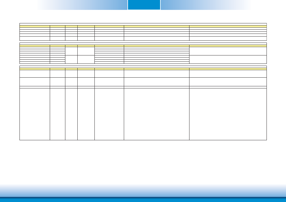
Signal
Pin#
Module Pin Type Pwr Rail /Tolerance
HU968
Carrier Board
Description
Power and System Management Signals Descriptions
ȟ
ȟ
ȟ
THRM#
B35
I CMOS
3.3V / 3.3V
PU 10K to 3.3V
Input from off-Module temp sensor indicating an over-temp situation.
THRMTRIP#
A35
O CMOS
3.3V / 3.3V
PU 10K to 3.3V
Active low output indicating that the CPU has entered thermal shutdown.
SMB_CK
B13
I/O OD CMOS
3.3V Suspend/3.3V
PU 2.2K to 3V3_DU_EC
System Management Bus bidirectional clock line.
SMB_DAT
B14
I/O OD CMOS
3.3V Suspend/3.3V
PU 2.2K to 3V3_DU_EC
System Management Bus bidirectional data line.
SMB_ALERT#
B15
I CMOS
3.3V Suspend/3.3V
System Management Bus Alert – active low input can be used to
generate an SMI# (System Management Interrupt) or to wake the system.
Signal
Pin#
Module Pin Type Pwr Rail /Tolerance
HU968
Carrier Board
Description
GPO0
A93
GPO1
B54
GPO2
B57
GPO3
B63
GPI0
A54
PU 100K to 3.3V
GPI1
A63
PU 100K to 3.3V
GPI2
A67
PU 100K to 3.3V
GPI3
A85
PU 100K to 3.3V
Signal
Pin#
Module Pin Type Pwr Rail /Tolerance
HU968
Carrier Board
Description
VCC_12V
A104~A109
B104~B109
C104~C109
D104~D109
Power
Primary power input: +12V nominal. All available VCC_12V pins on the connector(s) shall be used.
VCC_5V_SBY
B84~B87
Power
Standby power input: +5.0V nominal. If VCC5_SBY is used, all
available VCC_5V_SBY pins on the connector(s) shall be used. Only
used for standby and suspend functions. May be left unconnected if
these functions are not used in the system design.
VCC_RTC
A47
Power
Real-time clock circuit-power input. Nominally +3.0V.
GND
A1, A11, A21, A31,
A41, A51, A57, A60,
A66, A70, A80, A90,
A100, A110, B1,
B11, B21 ,B31, B41,
B51, B60, B70, B80,
B90, B100, B110,
C1, C2, C5, C8, C11,
C14, C21, C31, C41,
C51, C60, C70, C73,
C76, C80, C84, C87,
C90, C93, C96,
C100, C103, C110,
D1, D2, D5, D8,
D11, D14, D21,
D31, D51, D60,
D67, D70, D73,
D76, D80, D84,
D87, D90, D93,
D96, D100, D103,
D110
Power
Ground - DC power and signal and AC signal return path.
All available GND connector pins shall be used and tied to Carrier
Board GND plane.
Power and GND Signal Descriptions
I CMOS
3.3V / 3.3V
General purpose input pins.
Pulled high internally on the Module.
GPIO Signals Descriptions
O CMOS
General purpose output pins.
Upon a hardware reset, these outputs should be low.
3.3V / 3.3V