Chapter 3 – DFI KB968 User Manual
Page 22
www.dfi .com
Chapter 3 Hardware Installation
22
Chapter 3
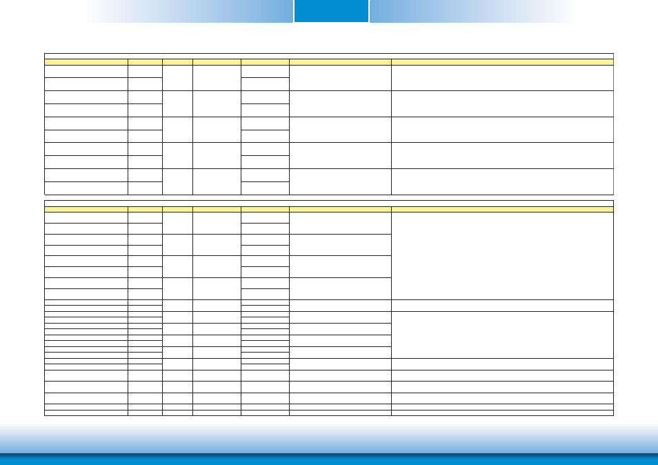
Signal
Pin#
Pin Type
Pwr Rail /Tolerance
KB968
Carrier Board
Description
ȟ
ȟ
ȟ
ȟ
USB Signals Descriptions
USB_SSRX1+
C7
USB_SSRX1-
C6
USB_SSTX2+
D10
NA
USB_SSTX2-
D9
NA
USB_SSRX2+
C10
NA
USB_SSRX2-
C9
NA
USB_SSTX3+
D13
NA
USB_SSTX3-
D12
NA
USB_SSRX3+
C13
NA
USB_SSRX3-
C12
NA
Signal
Pin#
Pin Type
Pwr Rail /Tolerance
KB968
Carrier Board
Description
LVDS_A0+
A71
LVDS_A0-
A72
LVDS_A1+
A73
LVDS_A1-
A74
LVDS_A2+
A75
LVDS_A2-
A76
LVDS_A3+
A78
NA
LVDS_A3-
A79
NA
LVDS_A_CK+
A81
LVDS_A_CK-
A82
LVDS_B0+
B71
NA
LVDS_B0-
B72
NA
LVDS_B1+
B73
NA
LVDS_B1-
B74
NA
LVDS_B2+
B75
NA
LVDS_B2-
B76
NA
LVDS_B3+
B77
NA
LVDS_B3-
B78
NA
LVDS_B_CK+
B81
NA
LVDS_B_CK-
B82
NA
LVDS_VDD_EN
A77
O CMOS
3.3V / 3.3V
Connect to enable control of LVDS panel power
circuit
LVDS panel power enable
LVDS_BKLT_EN
B79
O CMOS
3.3V / 3.3V
Connect to enable control of LVDS panel backlight
power circuit.
LVDS panel backlight enable
LVDS_BKLT_CTRL
B83
O CMOS
3.3V / 3.3V
Connect to brightness control of LVDS panel
backlight power circuit.
LVDS panel backlight brightness control
LVDS_I2C_CK
A83
I/O OD CMOS 3.3V / 3.3V
PU 4.7K to 3.3V
Connect to DDC clock of LVDS panel
I2C clock output for LVDS display use
LVDS_I2C_DAT
A84
I/O OD CMOS 3.3V / 3.3V
PU 4.7K to 3.3V
Connect to DDC data of LVDS panel
I2C data line for LVDS display use
ȟ
ȟ
ȟ
ȟ
I PCIE
AC coupled off Module
Additional receive signal differential pairs for the SuperSpeed USB data path.
O PCIE
NA
LVDS Channel A differential clock
O LVDS
LVDS
Connect to LVDS connector
O LVDS
NA
Connect 90ಳ @100MHz Common Choke in series
and ESD suppressors to GND to USB connector
NA
NA
NA
NA
LVDS Channel B differential pairs
Ther LVDS flat panel differential pairs (LVDS_A[0:3]+/-, LVDS_B[0:3]+/-. LVDS_A_CK+/-,
LVDS_B_CK+/-) shall have 100ƻ terminations across the pairs at the destination. These
terminations may be on the Carrier Board if the Carrier Board implements a LVDS deserializer
on-board
O LVDS
LVDS
NA
O LVDS
LVDS
NA
LVDS Signals Descriptions
O LVDS
LVDS
Connect to LVDS connector
LVDS Channel A differential pairs
Ther LVDS flat panel differential pairs (LVDS_A[0:3]+/-, LVDS_B[0:3]+/-. LVDS_A_CK+/-,
LVDS_B_CK+/-) shall have 100ƻ terminations across the pairs at the destination. These
terminations may be on the Carrier Board if the Carrier Board implements a LVDS deserializer
on-board
O LVDS
Connect to LVDS connector
O LVDS
LVDS
NA
LVDS
LVDS
Connect to LVDS connector
O LVDS
LVDS
O LVDS
LVDS
LVDS Channel B differential clock
O LVDS
LVDS
AC coupled on Module
Additional transmit signal differential pairs for the SuperSpeed USB data path.
I PCIE
AC coupled off Module
Additional receive signal differential pairs for the SuperSpeed USB data path.
O PCIE
AC coupled on Module
Additional transmit signal differential pairs for the SuperSpeed USB data path.
I PCIE
AC coupled off Module
Additional receive signal differential pairs for the SuperSpeed USB data path.
NA