Chapter 3 – DFI KB968 User Manual
Page 25
www.dfi .com
Chapter 3 Hardware Installation
25
Chapter 3
ȟ
ȟ
ȟ
ȟ
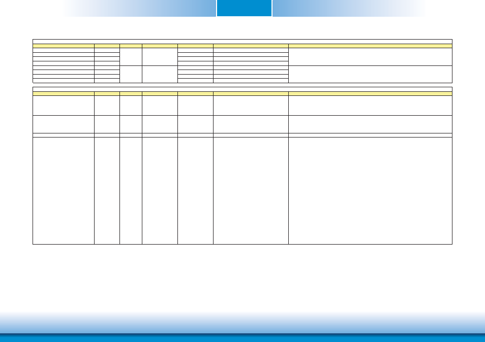
Signal
Pin#
Pin Type
Pwr Rail /Tolerance
KB968
Carrier Board
Description
GPO0
A93
GPO1
B54
GPO2
B57
GPO3
B63
GPI0
A54
PU 100K to 3.3V
GPI1
A63
PU 100K to 3.3V
GPI2
A67
PU 100K to 3.3V
GPI3
A85
PU 100K to 3.3V
Signal
Pin#
Pin Type
Pwr Rail /Tolerance
KB968
Carrier Board
Description
VCC_12V
A104~A109
B104~B109
C104~C109
D104~D109
Power
Primary power input: +12V nominal. All available VCC_12V pins on the connector(s) shall be used.
VCC_5V_SBY
B84~B87
Power
Standby power input: +5.0V nominal. If VCC5_SBY is used, all
available VCC_5V_SBY pins on the connector(s) shall be used. Only
used for standby and suspend functions. May be left unconnected if
these functions are not used in the system design.
VCC_RTC
A47
Power
Real-time clock circuit-power input. Nominally +3.0V.
GND
A1, A11, A21,
A31, A41, A51,
A57, A60, A66,
A70, A80, A90,
A100, A110, B1,
B11, B21 ,B31,
B41, B51, B60,
B70, B80, B90,
B100, B110, C1,
C2, C5, C8,
C11, C14, C21,
C31, C41, C51,
C60, C70, C73,
C76, C80, C84,
C87, C90, C93,
C96, C100,
C103, C110,
D1, D2, D5, D8,
D11, D14, D21,
D31, D51, D60,
D67, D70, D73,
D76, D80, D84,
D87, D90, D93,
D96, D100,
D103, D110
Power
Ground - DC power and signal and AC signal return path.
All available GND connector pins shall be used and tied to Carrier
Board GND plane.
Power and GND Signal Descriptions
I CMOS
3.3V / 3.3V
General purpose input pins.
GPIO Signals Descriptions
O CMOS
General purpose output pins.
3.3V / 3.3V