3 nand flash, 6 hssi or serdes block, Table 4-2 – Artesyn SCP-P4040-4G-ENP2 Installation and Use (August 2014) User Manual
Page 34: Nand flash map, Table 4-3, Functional description
Functional Description
SCP-P4040-4G-ENP2 Installation and Use (6806800P60B)
34
4.5.3
NAND Flash
The NAND FLASH is attached to the FCM on local bus and works at 8-bit mode.
The NAND FLASH is Micron MT29F8G08ADADAH4 whose FLASH size is 08 G bits or 1 G Bytes.
The pages are large and each page contains 2112 bytes including 2048 bytes of data and 64
bytes of spare. There are totally 8192 blocks, each block contains 64 pages including 128 KB of
data and 4 KB of spare.
The NAND FLASH is only used as NAND FLASH JFFS2 rootfs.The detailed map is described in the
following table:
4.6
HSSI OR SERDES Block
SCP-P4040-4G-ENP2 contains SERDES 3 banks including a total of 18 lanes. From the 18 lanes
of SERDES, 12 are routed to the COM Express connectors, defined as SERDES0~ SERDES7
(SERDES0~7 of bank 1) and SERDES16~SERDES19 (SERDES10~13 of bank 2).
SERDES8~SERDES9 of bank 1 are used for Aurora debugger defined as Aurora0~1.
The remaining 4 lanes of bank 3 are not used in P4040.
The protocol running at each lane or each group of lanes routed to COM Express connectors are
configured by the RCW, available options are shown in the following table:
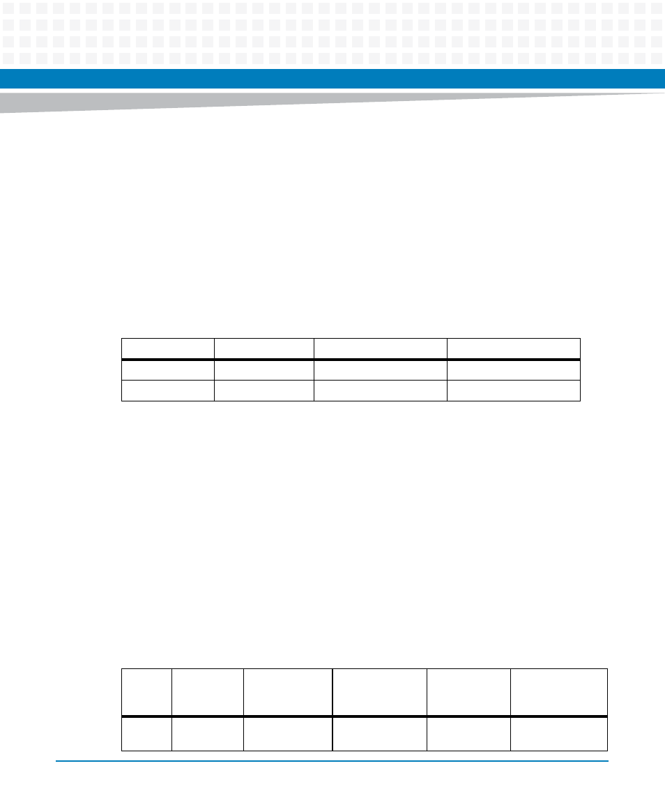
Table 4-2 NAND FLASH Map
Start Address
End Address
Size
Description
0000 0000
00FF FFFF
16 MB
Not Used
0100 0000
3FFF FFFF
1GB - 16MB
NAND FLASH JFFS2 rootfs
Table 4-3 Options of the SERDES routed to COM Express Connectors
Option
#
Bank1
SerDes 0 ~
3 (SLOT J6)
Bank1 SerDes
4 ~ 7 (SLOT J14)
Bank2 SerDes
10 ~ 13 (SLOT
J10)
RCW
[SRDS_PRTCL]
Bank 3# SerDes
14~17(slot J2)
1
PEX1 x4
(2.5Gbps)
PEX2 x4
(2.5Gbps)
XAUI
(3.125Gbps)
0x05
XAUI FM1 10 GEC