Differential mode pin naming convention, Altiobuf output buffer, Where – Altera I/O Buffer (ALTIOBUF) IP Core User Manual
Page 12: Is connected to the, Port, Port of the first oe delay chain port
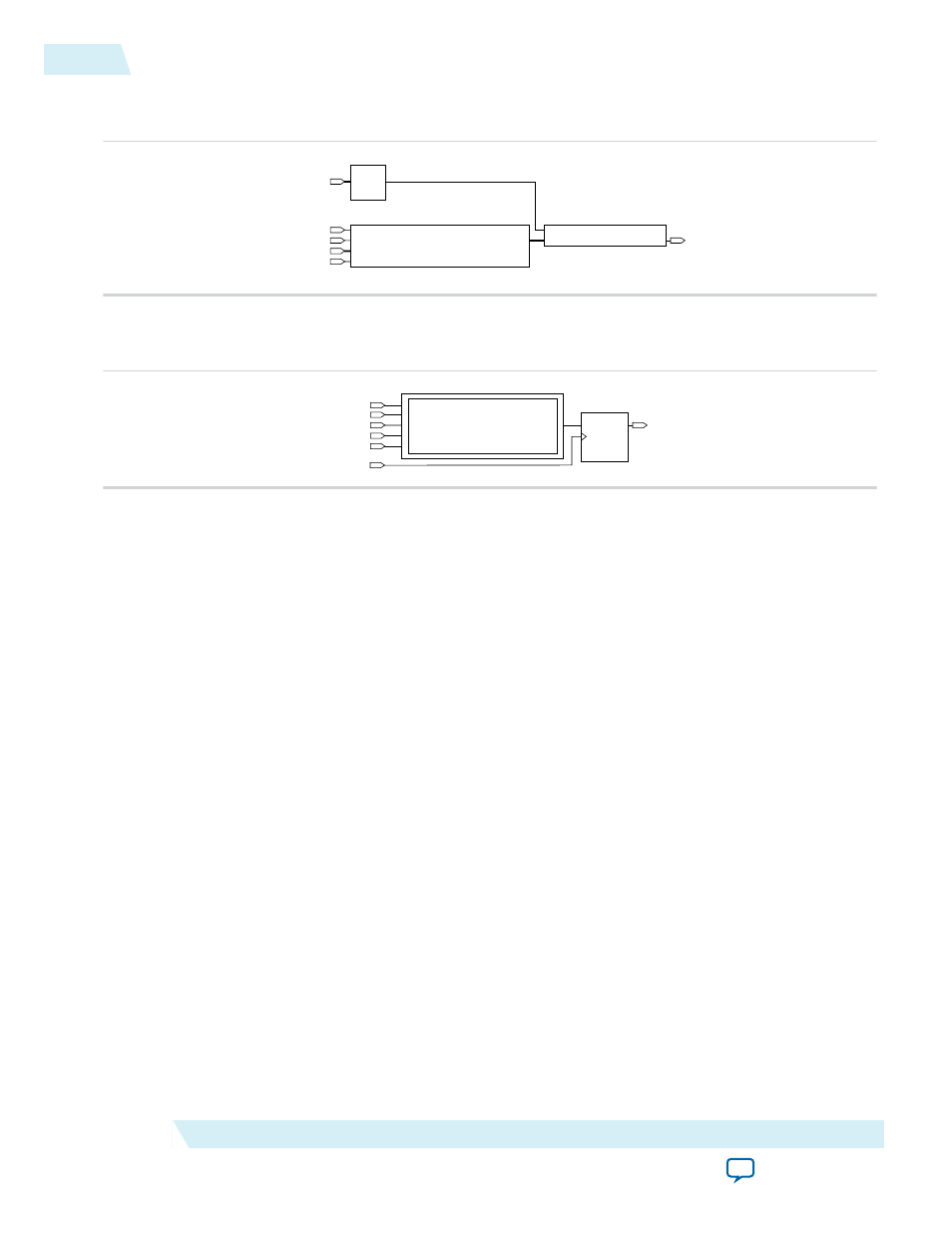
Figure 7: Internal Architecture of ALTIOBUF (Input Buffer Mode)
This figure shows the internal architecture of the input buffer in the ALTIOBUF IP core.
STRATIXIII_IO_IBUF
ibufa_0
I
O
datain[0..0]
io_config_datain
io_config_clk
ioconfiga_0
STRATIXIII_IO_CONFIG
io_config_clkena[0..0]
io_config_update
DATAIN
CLK
ENA
PADTOINPUTREGISTERDELAYSETTING[3..0]
UPDATE
STRATIXIII_DELAY_CHAIN
input_dyn_delay_chaina_0
DATAIN
DELAYCTRLIN[3..0]
DATAOUT
dataout[0..0]
Figure 8: ALTIOBUF (Input Buffer Mode) Connected to the External Flipflop
This figure shows how to connect the external register to the IP core.
io_config_datain
io_config_clk
inddc01_w1:altiobuf_in
datain
io_config_clkena
io_config_update
ffclk
dataout
io_config_clk
io_config_datain
io_config_update
dataout[0..0]
datain[0..0]
io_config_clkena[0..0]
PRN
CLR
D
Q
input_ff
ENA
Differential Mode Pin Naming Convention
Use the following pin naming convention for differential mode:
<pin_name>[1..0]
Where:
•
<pin_name>[0]
is connected to the
datain
port
•
<pin_name>[1]
is connected to the
datain_b
port.
Note: You must apply a differential I/O standard to both pins.
ALTIOBUF Output Buffer
The ALTIOBUF IP core (output buffer mode) uses the output and oe path of the dynamic delay chain,
where both share the same IO_CONFIG settings.
Contrary to the input path in the output and oe paths, you can add two optional registers, which are
external to the IP core. One is for the output path and the other is for the oe path.
Instead of connecting the input data to the
datain
port of the ALTIOBUF IP core (output buffer mode),
it is connected to the input of the registers that are external to the IP core. The output of the register is
then driven to the
datain
port of the first output delay chain port. In a similar way, the inverted input oe
is connected to the oe register that is external to the IP core, which drives the
datain
port of the first oe
delay chain port.
12
Differential Mode Pin Naming Convention
UG-01024
2014.12.15
Altera Corporation
I/O Buffer (ALTIOBUF) IP Core User Guide