Dynamic delay chain valid values, Is the name of the buffer, either a, For the output buffer) or – Altera I/O Buffer (ALTIOBUF) IP Core User Manual
Page 14
By following these specifications, only the input path needs a register external to the IP core. The output
and oe registers that are added externally to the IP core are optional.
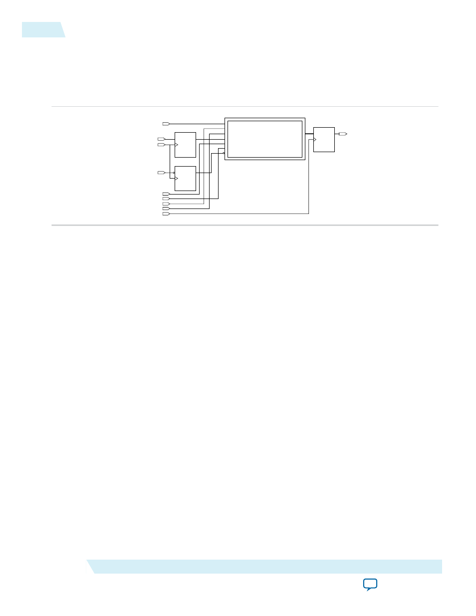
Figure 12: ALTIOBUF (Bidirectional Buffer Mode) Connected with External Flipflops
This figure shows an example of the ALTIOBUF IP core (bidirectional buffer mode) when output, oe, and
input path registers are used that are external to the IP core.
datain
io_config_clk
tc_bidir_01:altiobuf_bidir
oe
outffclk
dataout
io_config_clk
io_config_datain
io_config_update
dataout[0..0]
datain[0..0]
dataio[0..0]
PRN
CLR
D
Q
output_ff
ENA
PRN
CLR
D
Q
oe_ff
ENA
io_config_clkena[0..0]
io_config_clkena
dataio
io_config_datain
io_config_update
inffclk
oe[0..0]
PRN
CLR
D
Q
input_ff
ENA
The external register placement is similar to the input/output buffers, where the output and oe registers
drive the datain and oe ports of the ALTIOBUF IP core (bidirectional buffer mode) and the dataout port
drives the input register.
Note: • The dynamic termination control path also contains output delay chain 1 and output delay
chain 2, which are not accessible through the ALTIOBUF IP core (bidirectional buffer mode).
When both the oe and dynamic termination control are used, the two signals (oe and dynamic
termination control) can be out of synchronization.
• It is not recommended to switch these two signals simultaneously.
Dynamic Delay Chain Valid Values
For information about the delay chain valid values, refer to the Programmable IOE Delay section of the
respective device handbook or data sheet.
Assignments Necessary For Dynamic Delay Chain Usage
If you utilize the dynamic delay chain for the I/O buffer IP core, a
MEMORY_INTERFACE_DATA_PIN_GROUP
assignment to the I/O buffer block is necessary to enable it to go through fitting.
This is because the IP core utilizes the
IO_CONFIG
and
DELAY_CHAIN
blocks that are associated with the
use of DDR interfaces. Therefore, the Quartus II Fitter requires the assignment to determine the
placement of the blocks with the respective
IO_xBUF
block.
The format of the MEMORY_INTERFACE_DATA_PIN assignments generally appears as the following:
MEMORY_INTERFACE_DATA_PIN_GROUP {4|9|18|36} -from iobuf[0] -to iobuf[0]
MEMORY_INTERFACE_DATA_PIN_GROUP {4|9|18|36} -from iobuf[0] -to iobuf[1]
MEMORY_INTERFACE_DATA_PIN_GROUP {4|9|18|36} -from iobuf[0] -to iobuf[2]
….
MEMORY_INTERFACE_DATA_PIN_GROUP {4|9|18|36} -from iobuf[0] -to iobuf[n]
iobuf
is the name of the buffer, either a
stratixiii_io_obuf
(for the output buffer) or
stratixiii_io_ibuf
(for the input buffer). For the bidirectional buffer, either one is acceptable.
14
Dynamic Delay Chain Valid Values
UG-01024
2014.12.15
Altera Corporation
I/O Buffer (ALTIOBUF) IP Core User Guide