Altera I/O Buffer (ALTIOBUF) IP Core User Manual
Page 15
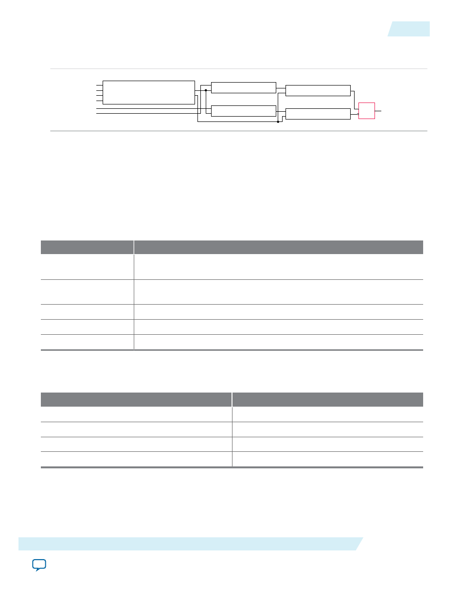
Figure 13: Output Buffer
This figure shows an example of an output buffer.
ioconfiga_0
obufa_0
output_dyn_delay_chain1a_0
oe_dyn_delay_chain1a_0
output_dyn_delay_chain2a_0
oe_dyn_delay_chain2a_0
DATAIN
CLK
ENA
UPDATE
OUTPUTDELAYSETTING1[3..0]
OUTPUTDELAYSETTING2[2..0]
DATAIN
DELAYCTRLIN[3..0]
DATAOUT
DATAIN
DELAYCTRLIN[3..0]
I
OE
O
DATAOUT
DATAIN
DELAYCTRLIN[3..0]
DATAOUT
DATAIN
DELAYCTRLIN[3..0]
DATAOUT
To allow this particular design to be fit, add the following line in the Quartus Setting File (.qsf):
set_instance_assignment -name MEMORY_INTERFACE_DATA_PIN_GROUP 4 -from "u2|
test_output_iobuffer_iobuf_out_kk21:test_output_iobuffer_iobuf_out_kk21_component|
obufa_0" -to "u2|
test_output_iobuffer_iobuf_out_kk21:test_output_iobuffer_iobuf_out_kk21_component|
obufa_0"
You can also use the Assignment Editor to set the column fields as shown in the following table:
Table 4: Assigning the MEMORY_INTERFACE_DATA_PIN_GROUP Assignment
Column
Setting
From
u2|test_output_iobuffer_iobuf_out_kk21:test_output_iobuffer_iobuf_
out_kk21_component|obufa_0
To
u2|test_output_iobuffer_iobuf_out_kk21:test_output_iobuffer_iobuf_
out_kk21_component|obufa_0
Assignment Name
MEMORY_INTERFACE_DATA_PIN_GROUP
Value
4
Enable
Yes
Then, set the Value field as shown in the following table:
Table 5: MEMORY_INTERFACE_DATA_PIN_GROUP Value
Number of Channels
MEMORY_INTERFACE_DATA_PIN_GROUP Value
1–6
4
7–12
9
13–24
18
25–48
36
The design example associated with this user guide has this assignment.
Related Information
Provides the I/O configuration block bit sequence for Arria V, Cyclone V, and Stratix V devices
UG-01024
2014.12.15
Assignments Necessary For Dynamic Delay Chain Usage
15
I/O Buffer (ALTIOBUF) IP Core User Guide
Altera Corporation