Altiobuf bidirectional buffer – Altera I/O Buffer (ALTIOBUF) IP Core User Manual
Page 13
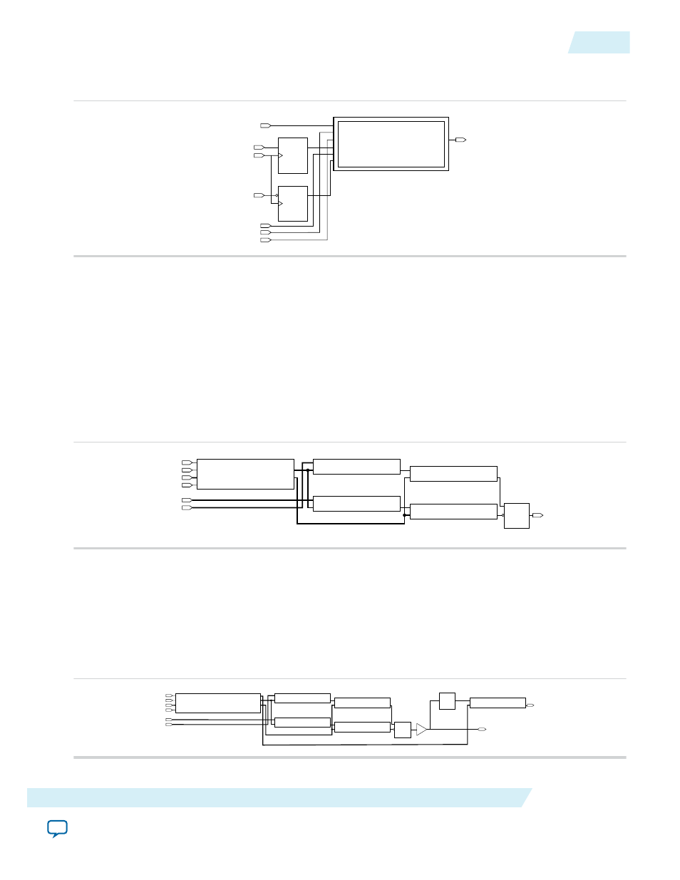
Figure 9: ALTIOBUF (Output Buffer Mode) Connected with the External Flipflops
This figure shows how to connect the output and oe registers to the ALTIOBUF IP core.
datain
io_config_clk
tc_out01:altiobuf_out
oe
outffclk
dataout
io_config_clk
io_config_datain
io_config_update
dataout[0..0]
datain[0..0]
io_config_clkena[0..0]
PRN
CLR
D
Q
output_ff
ENA
PRN
CLR
D
Q
oe_ff
ENA
oe[0..0]
io_config_datain
io_config_clkena
io_config_update
Each of the output and oe delay chains are built from two cascaded output delay chains. The first output
delay chain’s
dataout
is connected to the second output delay chain’s datain. Depending on the
parameter chosen (
use_out_dynamic_delay_chain1
or
use_out_dynamic_delay_chain2
), one or both
of the output delay chains can be dynamic. In this IP core, you can set the delay only for the dynamic
delay chains.
The second output delay chain’s
dataout
is connected to the output buffer’s i input port for the output
path and to the output buffer’s oe port for the oe path. Note that the output path and the oe path have
their own cascaded delay chains.
Figure 10: Internal Architecture of ALTIOBUF (Output Buffer Mode)
This figure shows the internal architecture of the ALTIOBUF IP core.
io_config_datain
io_config_clk
ioconfiga_0
STRATIXIII_IO_CONFIG
STRATIXIII_DELAY_CHAIN
STRATIXIII_DELAY_CHAIN
STRATIXIII_DELAY_CHAIN
STRATIXIII_DELAY_CHAIN
STRATIXIII_IO_OBUF
io_config_clkena[0..0]
io_config_update
dataout[0..0]
oe[0..0]
datain[0..0]
DATAIN
CLK
ENA
OUTPUTDELAYSETTING[3..0]
OUTPUTDELAYSETTING[2..0]
UPDATE
output_dyn_delay_chain2a_0
output_dyn_delay_chain1a_0
DATAIN
DELAYCTRLIN[3..0]
DATAOUT
oe_dyn_delay_chain1a_0
DATAIN
DELAYCTRLIN[3..0]
DATAOUT
obufa_0
DATAIN
DELAYCTRLIN[3..0]
DATAOUT
oe_dyn_delay_chain2a_0
DATAIN
DELAYCTRLIN[3..0]
I
OE
DATAOUT
O
ALTIOBUF Bidirectional Buffer
The bidirectional buffer essentially combines the input buffer and the output buffer, incorporating the
input path, output path, and oe path.
By combining the input and output buffers, the output path and oe path are placed before the buffer and
the input path is placed after the buffer.
Figure 11: Internal Architecture of ALTIOBUF (Bidirectional Buffer Mode)
ioconfiga_0
STRATIXIII_IO_CONFIG
STRATIXIII_DELAY_CHAIN
STRATIXIII_DELAY_CHAIN
STRATIXIII_DELAY_CHAIN
STRATIXIII_DELAY_CHAIN
STRATIXIII_IO_OBUF
DATAIN
CLK
ENA
OUTPUTDELAYSETTING[3..0]
PADTOINPUTREGISTERDELAYSETTING[3..0]
OUTPUTDELAYSETTING[2..0]
UPDATE
output_dyn_delay_chain2a_0
output_dyn_delay_chain1a_0
DATAIN
DELAYCTRLIN[3..0] DATAOUT
oe_dyn_delay_chain1a_0
DATAIN
DELAYCTRLIN[3..0] DATAOUT
obufa_0
DATAIN
DELAYCTRLIN[3..0] DATAOUT
oe_dyn_delay_chain2a_0
DATAIN
DELAYCTRLIN[3..0]
I
OE
DATAOUT
O
STRATIXIII_IO_IBUF
ibufa_0
I
O
STRATIXIII_DELAY_CHAIN
input_dyn_delay_chaina_0
DATAIN
DELAYCTRLIN[3..0] DATAOUT
dataio 1
UG-01024
2014.12.15
ALTIOBUF Bidirectional Buffer
13
I/O Buffer (ALTIOBUF) IP Core User Guide
Altera Corporation