Altera Signal Integrity Development Kit, Stratix V GX Edition User Manual
Page 16
4–4
Chapter 4: Development Board Setup
Factory Default Switch Settings
Transceiver Signal Integrity Development Kit
July 2012
Altera Corporation
Stratix V GX Edition User Guide
3. Set DIP switch bank (SW4) to match
4. Set DIP switch bank (SW5) to match
5. Set DIP switch bank (SW6) to match
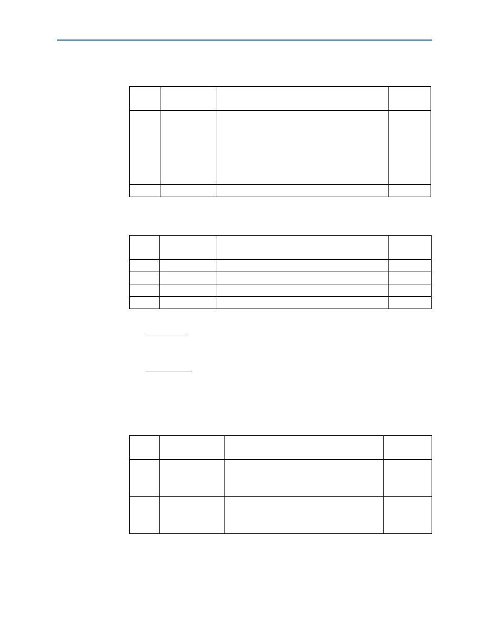
Table 4–3. SW4 User Dip Switch Settings
Switch
Board
Label
Function
Default
Position
1
S5_UNLOCK
Switch 1 has the following options:
■
Closed = FACTORY command won’t be issued. JTAG
will be locked out if FPGA is configured on power-up
from flash.
■
Open = Unlock the FPGA and allow FACTORY
command. JTAG will be available even if FPGA is
configured on power-up from flash.
Open
2–8
DPI6—DPI0
User defined options.
—
Table 4–4. SW5 Dip Switch Settings
Switch
Board
Label
Function
Default
Position
1
S0
Determines S5GX_CKL11 frequency.
1
2
S1
Determines S5GX_CKL11 frequency.
0
3
SS0
Determines S5GX_CKL11 spectrum spread.
0
4
SS1
Determines S5GX_CKL11 spectrum spread.
0
(1) Truth tables for the SW5 settings:
S1 S0 Frequency
00 25 MHz
01 100 MHz (default)
10 125 MHz
11 200 MHz
SS1 SS0 Spread%
00 center =/- 25%
01 down -0.5%
10 down -0.75%
11 no spread (default)
Table 4–5. SW6 Dip Switch Settings (Part 1 of 2)
Switch
Board
Label
Function
Default
Position
1
REFCLK_SEL_U32
Switch 1 has the following options:
■
When set at OSC, enables oscillator input.
■
When set at SMA, enables SMA input.
OSC
2
REFCLK_SEL_U33
Switch 2 has the following options:
■
When set at OSC, enables oscillator input.
■
When set at SMA, enables SMA input.
OSC