A. programming the flash memory device, Cfi flash memory map, Appendix a. programming the flash memory device – Altera Signal Integrity Development Kit, Stratix V GX Edition User Manual
Page 45: Table a–1
July 2012
Altera Corporation
Transceiver Signal Integrity Development Kit
Stratix V GX Edition User Guide
A. Programming the Flash Memory
Device
As you develop your own project using the Altera tools, you can program the flash
memory device so that your own design loads from flash memory into the FPGA on
power up. This appendix describes the preprogrammed contents of the common flash
interface (CFI) flash memory device on the Stratix V GX transceiver signal integrity
development board and the Nios II EDS tools involved with reprogramming the user
portions of the flash memory device.
The Stratix V GX transceiver signal integrity development board ships with the CFI
flash device preprogrammed with a default factory FPGA configuration for running
the Board Update Portal design example and a default user configuration for running
the Board Test System demonstration. There are several other factory software files
written to the CFI flash device to support the Board Update Portal. These software
files were created using the Nios II EDS, just as the hardware design was created
using the Quartus II software.
f
For more information about Altera development tools, refer to the
page of the Altera website.
CFI Flash Memory Map
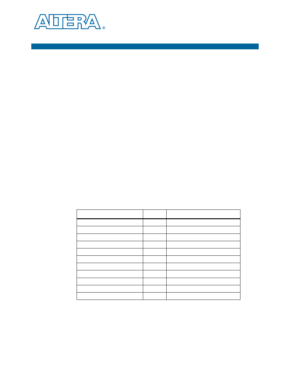
Table A–1 shows the default memory contents of the 1-Gb CFI flash device. For the
Board Update Portal to run correctly and update designs in the user memory, this
memory map must not be altered.
c
Altera recommends that you do not overwrite the factory hardware and factory
software images unless you are an expert with the Altera tools. If you unintentionally
overwrite the factory hardware or factory software image, refer to
Flash Device to the Factory Settings” on page A–4
Table A–1. Byte Address Flash Memory Map
Block Description
Size (KB)
Address Range
Unused
128
0x07FE.0000 - 0x07FF.FFFF
User software
24,320
0x0716.0000 - 0x07FD.FFFF
Factory software
8,192
0x0696.0000 - 0x0715.FFFF
Zipfs (html, web content)
8,192
0x0616.0000 - 0x0695.FFFF
User hardware 2
33,152
0x0410.0000 - 0x0615.FFFF
User hardware 1
33,152
0x020A.0000 - 0x040F.FFFF
Factory hardware
33,152
0x0002.0000 - 0x0209.FFFF
PFL option bits
32
0x0001.8000 - 0x0001.FFFF
Board information
32
0x0001.0000 - 0x0001.7FFF
Ethernet option bits
32
0x0000.8000 - 0x0000.FFFF
User design reset vector
32
0x0000.0000 - 0x0000.7FFF