The clock control, The clock control –21 – Altera Signal Integrity Development Kit, Stratix V GX Edition User Manual
Page 41
Chapter 6: Board Test System
6–21
The Clock Control
July 2012
Altera Corporation
Transceiver Signal Integrity Development Kit
Stratix V GX Edition User Guide
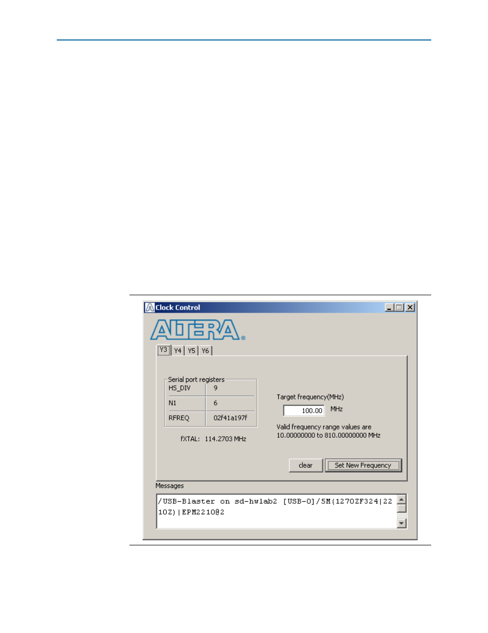
The Clock Control
The Clock Control application sets the Si570 programmable oscillator to any
frequency between 10 MHz and 945 MHz and select frequencies to 1400 MHz. The
oscillator drives a 2-to-4 buffer that drives a copy of the clock to all four edges of the
FPGA.
The Clock Control application runs as a stand-alone application. ClockControl.exe
resides in the
<install dir>\kits\stratixVGX_5sgxea7nf40_si\examples\board_test_system
directory.
On Windows, click Start > All Programs > Altera > Transceiver Signal Integrity
Development Kit, Stratix V GX Edition
<version> > Clock Control to start the
application.
f
For more information about the Si570 and the Stratix V GX transceiver signal integrity
development board’s clocking circuitry and clock input pins, refer to the
.
The Clock Control communicates with the MAX II device on the board through the
JTAG bus. The Si570 programmable oscillator is connected to the MAX II device
through a 2-wire serial bus.
shows the Clock Control.
The following sections describe the Clock Control controls.
Figure 6–10. The Clock Control