Components and interfaces, Pci express, Components and interfaces –24 – Altera Cyclone V SoC Development Board User Manual
Page 32: Pci express –24
2–24
Chapter 2: Board Components
Components and Interfaces
Cyclone V SoC Development Board
November 2013
Altera Corporation
Reference Manual
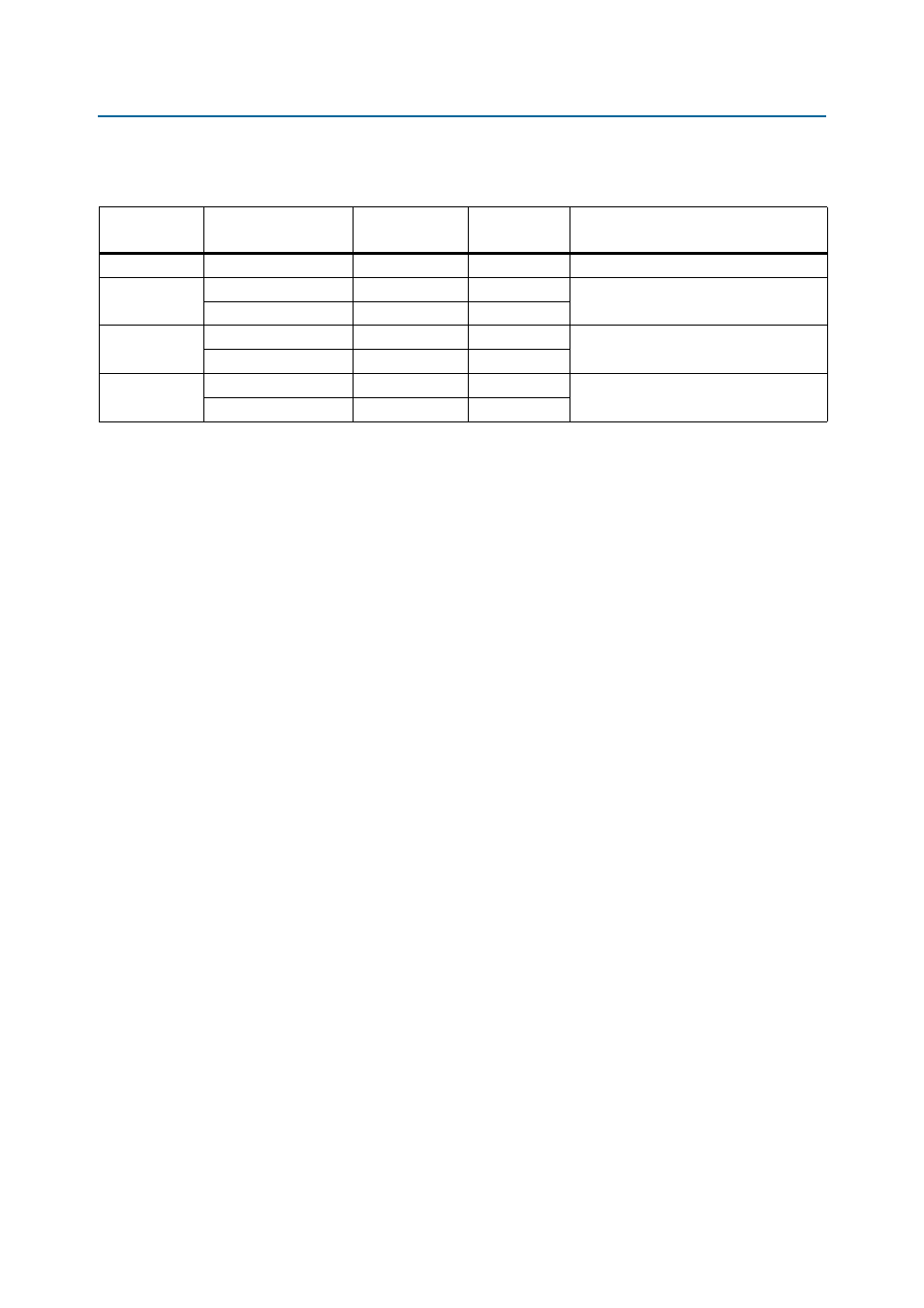
Table 2–17
lists the clock outputs for the development board.
Components and Interfaces
This section describes the development board's communication ports and interface
cards relative to the Cyclone V SoC device. The development board supports the
following communication ports:
■
PCI Express
■
10/100/1000 Ethernet (HPS)
■
10/100 Ethernet (FPGA)
■
HSMC
■
RS-232 Serial UART (HPS)
■
CAN bus (HPS)
■
Real-Time clock (HPS)
■
SPI master
■
I
2
C
■
SDI video
PCI Express
The PCI Express interface on the development board supports auto-negotiating
channel width from ×1 to ×4 as well as the connection speed of Gen1 at 2.5 Gbps/lane
for a maximum of 10 Gbps bandwidth.
The PCIE_REFCLK_P/N signal is a 100-MHz differential input that is driven to the
daughter card through the PCI Express edge connector. This signal connects directly
to a Cyclone V SoC REFCLK input pin pair using DC coupling. The I/O standard is
High-Speed Current Steering Logic (HCSL).
Table 2–17. Off-Board Clock Outputs
Source
Schematic Signal
Name
I/O Standard
Cyclone V SoC
Pin Number
Description
Samtec HSMC
HSMA_CLK_OUT0
2.5-V CMOS
A10
FPGA CMOS output (or GPIO)
Samtec HSMC
HSMA_CLK_OUT_P1
2.5-V CMOS
AJ2
CMOS output
HSMA_CLK_OUT_N1
2.5-V CMOS
AC12
Samtec HSMC
HSMA_CLK_OUT_P2
LVDS/2.5V CMOS
E7
LVDS output. Can also support 2x CMOS
outputs.
HSMA_CLK_OUT_N2
LVDS/2.5V CMOS
E6
PCI Express
Socket
PCIE_REFCLK_QL0_P
HCSL
W8
HCSL output to the PCI Express socket
PCIE_REFCLK_QL0_N
HCSL
W7