Real-time clock (hps), Spi master, I2c interface – Altera Cyclone V SoC Development Board User Manual
Page 43: Real-time clock (hps) –35 spi master –35 i, C interface
Chapter 2: Board Components
2–35
Components and Interfaces
November 2013
Altera Corporation
Cyclone V SoC Development Board
Reference Manual
lists the PHY device pin assignments, signal names, and functions. The
signal names and types are relative to the Cyclone V SoC in terms of I/O setting and
direction.
Real-Time Clock (HPS)
The HPS system has a battery backed real-time clock (RTC) connected through the I
2
C
interface. The RTC is implemented using a DS1339 device from Maxim
Semiconductor. The device has a built-in power sense circuit that detects power
failures and automatically switches to backup battery supply, maintaining time. The
device uses a 357 coin battery with a nominal voltage of 1.55 V. Using typical current
capacity, the RTC is expected to have 120,000 backup hours. The battery is mounted
inside a holder attached to the board to allow battery replacement or removal.
lists the RTC device pin assignments, signal names, and functions. The
signal names and types are relative to the Cyclone V SoC in terms of I/O setting and
direction.
SPI Master
The HPS system has a SPI master interface available on the board. This interface
connects to the Linear Technology expansion header (J31). This header can power and
interface to most Linear Technology daughter boards such as the included DC934
Dual D/A and A/D board.
I
2
C Interface
The HPS system has one I
2
C interface for communicating with the on-board and
external components. The data rate is 50kbps.
lists the I
2
C interface address map.
Table 2–25. PHY Device Schematic Signal Names and Functions
Board
Reference (U50)
Schematic Signal
Name
Cyclone V SoC
Pin Number
I/O Standard
Description
7
CANH_P
—
3.3-V
CAN bus line high
6
CANL_N
—
3.3-V
CAN bus line low
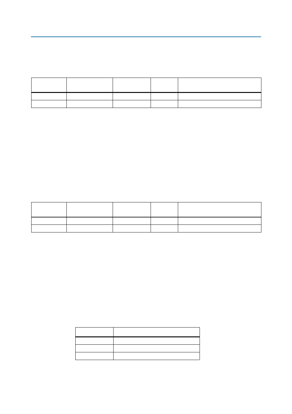
Table 2–26. RTC Device Schematic Signal Names and Functions
Board
Reference (U50)
Schematic Signal
Name
Cyclone V SoC
Pin Number
I/O Standard
Description
16
I2C_SDA_HPS
C23
3.3-V
Management serial data
1
I2C_SCL_HPS
D22
3.3-V
Management serial clock
Table 2–27. I
2
C interface address map
Address
Device
0x68
Real-time clock
0x50
LCD
0x5C
FPGA power monitor