Epcq flash, Cfi flash, Epcq flash –46 cfi flash –46 – Altera Cyclone V SoC Development Board User Manual
Page 54
2–46
Chapter 2: Board Components
Memory
Cyclone V SoC Development Board
November 2013
Altera Corporation
Reference Manual
EPCQ Flash
The development board supports one 256-Mb serial/quad-serial NOR flash device for
non-volatile storage of the FPGA configuration image. The device connects to the
FPGA dedicated interface through the IDTQS3861 device.
lists the EPCQ flash pin assignments, signal names, and functions. The
signal names and types are relative to the MAX V CPLD 5M2210 System Controller in
terms of I/O setting and direction. Some pins are used in other interfaces as well due
to functionality sharing.
CFI Flash
The development board supports a 512-Mb CFI-compatible synchronous flash device
for non-volatile storage of FPGA configuration data. This device connects to the
MAX V CPLD 5M2210 System Controller for FPGA configuration in FPP and PS
modes.
This 16-bit data memory interface can sustain burst read operations at up to 52 MHz
for a throughput of 832 Mbps per device. The write performance is 270 µs for a single
word buffer while the erase time is 800 ms for a 128 K array block.
Table 2–36
lists the flash pin assignments, signal names, and functions. The signal
names and types are relative to the MAX V CPLD 5M2210 System Controller in terms
of I/O setting and direction.
7
QSPI_SS0
A18
3.3-V Chip
enable
3
QSPI_RESETN
—
3.3-V
Reset (driven from the MAX V CPLD)
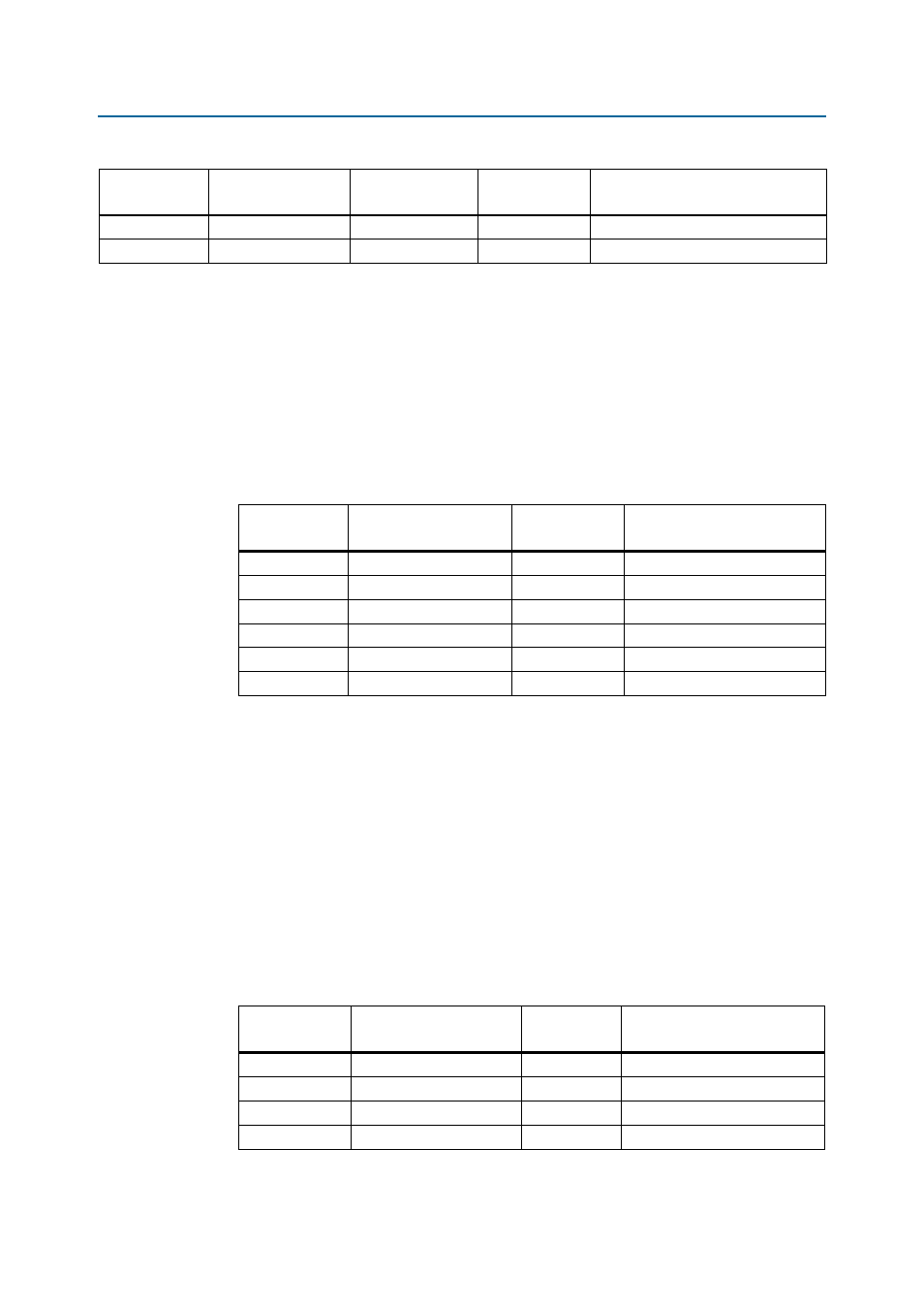
Table 2–34. QSPI Flash Schematic Signal Names and Functions
Board
Reference (U5)
Schematic
Signal Name
Cyclone V SoC Pin
Number
I/O Standard
Description
Table 2–35. EPCQ Flash Schematic Signal Names and Functions
Board
Reference (U20)
Schematic Signal Name
I/O Standard
Description
16
FPGA_DCLK
3.3-V Clock
15
FPGA_AS_DATA0
3.3-V Data
bus
8
FPGA_AS_DATA1
3.3-V Data
bus
9
FPGA_AS_DATA2
3.3-V Data
bus
1
FPGA_AS_DATA3
3.3-V Data
bus
7
FPGA_NCS0
3.3-V Chip
enable
Table 2–36. Flash Pin Assignments, Schematic Signal Names, and Functions (Part 1 of 3)
Board
Reference (U6)
Schematic Signal Name
I/O Standard
Description
F6
FLASH_ADVN
1.8-V
Address valid
B4
FLASH_CEN0
1.8-V
Chip enable
E6
FLASH_CLK
1.8-V
Clock
F8
FLASH_OEN
1.8-V
Output enable