Qspi flash (hps), Qspi flash (hps) –45 – Altera Cyclone V SoC Development Board User Manual
Page 53
Chapter 2: Board Components
2–45
Memory
November 2013
Altera Corporation
Cyclone V SoC Development Board
Reference Manual
QSPI Flash (HPS)
The development board supports one 512-Mb quad-SPI (QSPI) flash device for non-
volatile storage of the HPS boot code, user data, and program. The device connects to
the HPS dedicated interface. The device interface may contain a secondary boot code.
This 4-bit data memory interface can sustain burst read operations at up to 108 MHz
for a throughput of 54 MBps. Erase capability is at 4 KB, 64 KB, and 32 MB.
lists the QSPI flash pin assignments, signal names, and functions. The
signal names and types are relative to the Cyclone V SoC in terms of I/O setting and
direction.
F2
DDR3_HPS_DQ7
J29
1.5-V SSTL Class I
Data bus
C8
DDR3_HPS_DQ8
K26
1.5-V SSTL Class I
Data bus
B8
DDR3_HPS_DQ9
L26
1.5-V SSTL Class I
Data bus
D7
DDR3_HPS_DQ10
K29
1.5-V SSTL Class I
Data bus
A7
DDR3_HPS_DQ11
K27
1.5-V SSTL Class I
Data bus
C2
DDR3_HPS_DQ12
M26
1.5-V SSTL Class I
Data bus
C3
DDR3_HPS_DQ13
M27
1.5-V SSTL Class I
Data bus
A3
DDR3_HPS_DQ14
L28
1.5-V SSTL Class I
Data bus
A2
DDR3_HPS_DQ15
M30
1.5-V SSTL Class I
Data bus
G3
DDR3_HPS_DQS_N0
M19
Differential 1.5-V
SSTL Class I
Data strobe P byte lane 0
B7
DDR3_HPS_DQS_N1
N24
Differential 1.5-V
SSTL Class I
Data strobe N byte lane 0
F3
DDR3_HPS_DQS_P0
N18
Differential 1.5-V
SSTL Class I
Data strobe P byte lane 1
C7
DDR3_HPS_DQS_P1
N25
Differential 1.5-V
SSTL Class I
Data strobe N byte lane 1
K1
DDR3_HPS_ODT
H28
1.5-V SSTL Class I
On-die termination enable
J3
DDR3_HPS_RASN
D30
1.5-V SSTL Class I
Row address select
T2
DDR3_HPS_RESETN
P30
1.5-V SSTL Class I
Reset
L3
DDR3_HPS_WEN
C28
1.5-V SSTL Class I
Write enable
L8
DDR3_HPS_ZQ
—
1.5-V SSTL Class I
ZQ impedance calibration
Table 2–33. DDR3 SDRAM Pin Assignments, Schematic Signal Names, and Functions (Part 5 of 5)
Board
Reference
Schematic
Signal Name
Cyclone V SoC
Pin Number
I/O Standard
Description
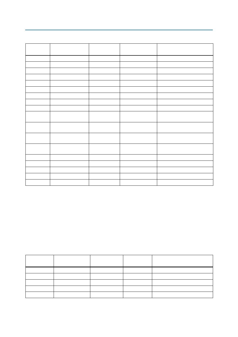
Table 2–34. QSPI Flash Schematic Signal Names and Functions
Board
Reference (U5)
Schematic
Signal Name
Cyclone V SoC Pin
Number
I/O Standard
Description
16
QSPI_CLK
D19
3.3-V Clock
15
QSPI_IO0
C20
3.3-V Data
bus
8
QSPI_IO1
H18
3.3-V Data
bus
9
QSPI_IO2
A19
3.3-V Data
bus
1
QSPI_IO3
E19
3.3-V Data
bus