Block diagram, Default reference design – Altera Nios Development Board User Manual
Page 10
1–2
Altera
Corporation
Nios Development Board Reference Manual, Cyclone Edition
December 2004
General Description
f
See the Nios II Development Kit, Getting Started User Guide for instructions
on setting up the Nios development board and installing Nios II
development tools.
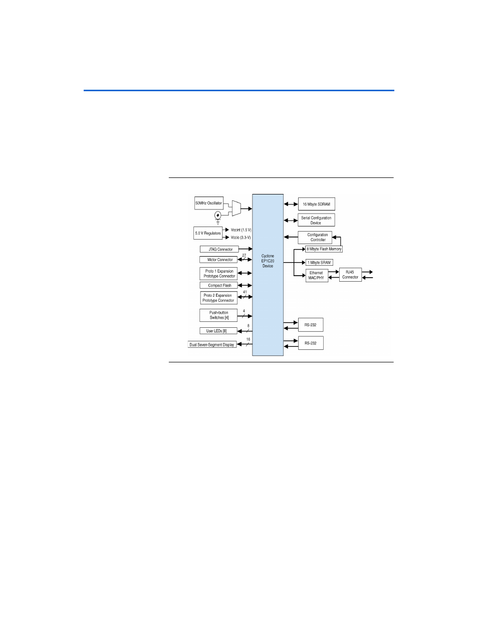
Block Diagram
shows a block diagram of the board.
Figure 1–1. Nios Development Board, Cyclone Edition Block Diagram
Default Reference Design
When power is applied to the board, the on-board logic configures the
Cyclone FPGA using hardware configuration data stored in flash
memory. When the device is configured, the Nios II processor design in
the FPGA wakes up and begins executing boot code from flash memory.
The board is factory-programmed with a default reference design. This
reference design is a web server that delivers web pages via the Ethernet
port. For further information on the default reference design, see
Appendix C, Connecting to the Board via Ethernet
.