Appendix a. shared bus table, Description – Altera Nios Development Board User Manual
Page 41
Altera Corporation
A–1
December 2004
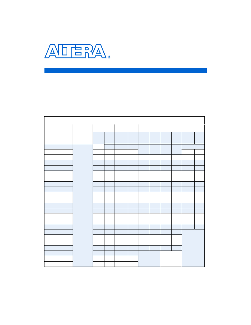
Appendix A. Shared Bus Table
Description
On the Nios development board, Cyclone Edition, the flash memory,
SRAM, and Ethernet MAC/PHY devices share address and control lines.
These shared lines are referred to as the Shared Bus. Using SOPC Builder,
designers can interface a Nios II processor system to any device
connected to the off-chip Shared Bus.
lists all
connections between the devices connected to the Shared Bus.
Table A–9. Shared Bus Table (Part 1 of 3)
NET Name
NET
Description
PLD (U60)
Flash (U5)
SRAM (U35) SRAM (U36) Ethernet (U4)
Pin
Name
Pin #
Pin
Name
Pin #
Pin
Name
Pin #
Pin
Name
Pin #
Pin
Name
Pin #
FSE_A0
Shared
Address
IO
B4
A0
27
FSE_A1
IO
A4
A1
22
A1
78
FSE_A2
IO
D5
A2
21
A0
1
A0
1
A2
79
FSE_A3
IO
D6
A3
20
A1
2
A1
2
A3
80
FSE_A4
IO
C5
A4
19
A2
3
A2
3
A4
81
FSE_A5
IO
B5
A5
18
A3
4
A3
4
A5
82
FSE_A6
IO
C2
A6
17
A4
5
A4
5
A6
83
FSE_A7
IO
D2
A7
16
A5
18
A5
18
A7
84
FSE_A8
IO
D4
A8
10
A6
19
A6
19
A8
85
FSE_A9
IO
D1
A9
9
A7
20
A7
20
A9
86
FSE_A10
IO
E4
A10
42
A8
21
A8
21
A10
87
FSE_A11
IO
E5
A11
8
A9
22
A9
22
A11
88
FSE_A12
IO
F3
A12
7
A10
23
A10
23
A12
89
FSE_A13
IO
E3
A13
6
A11
24
A11
24
A13
90
FSE_A14
IO
E2
A14
5
A12
25
A12
25
A14
91
FSE_A15
IO
F4
A15
4
A13
26
A13
26
A15
92
FSE_A16
IO
F5
A16
3
A14
27
A14
27
FSE_A17
IO
F2
A17
46
A15
42
A15
42
FSE_A18
IO
F1
A18
15
A16
43
A16
43
FSE_A19
IO
F6
A19
43
A17
44
A17
44
FSE_A20
IO
G5
A20
44
FSE_A21
IO
G1
A21
35
FSE_A22
IO
G2
A22
2