Sdram device, Sdram device –8 – Altera Nios Development Board User Manual
Page 16
1–8
Altera
Corporation
Nios Development Board Reference Manual, Cyclone Edition
December 2004
SDRAM Device
f
For more information on the CompactFlash connector (CON3), see
www.compactflash.org
and www.molex.com.
SDRAM Device
The SDRAM device (U57) is a Micron MT48LC4M32B2 chip with PC100
functionality and self refresh mode. The SDRAM is fully synchronous
with all signals registered on the positive edge of the system clock.
33
-VS1
GND
(3)
34
-OIORD
G19
35
-IOWR
G20
36
-WE
V18
37
RDY/BSY
G17
38
VCC
M13
(2)
39
-CSEL
GND
(3)
40
-VS2
no connect
(3)
41
RESET
(4)
42
-WAIT
G14
43
-INPACK
V19
44
-REG
U20
45
BVD2
J16
46
BVD1
J19
47
D081
C19
48
D091
D19
49
D101
D20
50
GND
GND
(3)
Note to
(1)
All pin numbers represent I/O pins on the FPGA, unless
otherwise noted.
(2)
This FPGA I/O pin controls a power MOSFET that supplies 5V
VCC to CON3.
(3)
This pin does not connect to the FPGA directly.
(4)
RESET is driven by the EPM7128AE configuration controller
device.
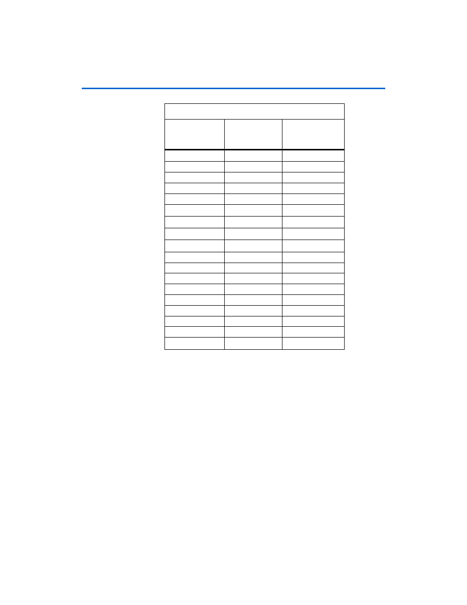
Table 1–2. CompactFlash (CON3) Pin Table
Pin on
CompactFlash
(CON3)
CompactFlash
Function
Connects to
(1)