Power-supply circuitry, Clock circuitry, Power-supply circuitry –28 clock circuitry –28 – Altera Nios Development Board User Manual
Page 36
1–28
Altera
Corporation
Nios Development Board Reference Manual, Cyclone Edition
December 2004
Power-Supply Circuitry
Power-Supply
Circuitry
The Nios development board runs from a 9-V, unregulated, center-
negative input power supply. On-board circuitry generates 5-V, 3.3-V, and
1.5-V regulated power levels.
■
The 5-V supply is present on pin 2 of J12 and J15 for use by any device
plugged into the PROTO1 or PROTO2 expansion connectors.
■
The 3.3-V supply is used as the power source for all Cyclone device
I/O pins. The 3.3-V supply is also available to PROTO1 and PROTO2
daughter cards.
■
The 1.5-V supply is used only as the power supply for the Cyclone
device core (VCCINT) and it is not available on any connector or
header.
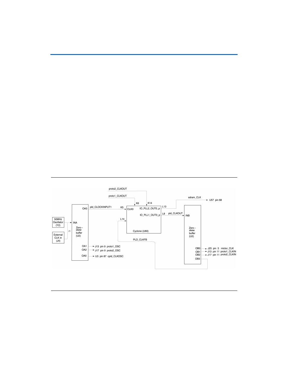
Clock Circuitry
The Nios development board includes a
50 MHz free-running oscillator
and a zero-skew, point-to-point clock distribution network. The clock
network drives the Cyclone device and pins on the expansion prototype
connectors, the configuration controller device, and the Mictor connector.
The zero-skew buffer distributes both the free-running
50 MHz clock and
the clock-output from one of the Cyclone's device internal PLLs
(CLKLK_OUT1). See
Figure 1–21. Clock Circuitry
Note to
(1)
An external clock can be enabled by stuffing location R15 with a 49.9 ohm 0603 resistor and stuffing location R13
with a 330 ohm 0603 resistor.