Programming nand flash – Altera Parallel Flash Loader IP User Manual
Page 12
Programming NAND Flash
You can use the JTAG interface in Altera CPLDs to program the NAND flash memory device with the
PFL IP core. The NAND flash memory device is a simpler device that has faster erase and write speed with
higher memory density in comparison with the CFI flash.
You can use the JTAG interface in Altera CPLDs to indirectly program the flash memory device. The
CPLD JTAG block interfaces directly with the logic array in a special JTAG mode. This mode brings the
JTAG chain through the logic array instead of the Altera CPLD BSCs. The PFL IP core provides JTAG
interface logic to convert the JTAG stream from the Quartus II software and to program the NAND flash
memory device that connects to the CPLD I/O pins.
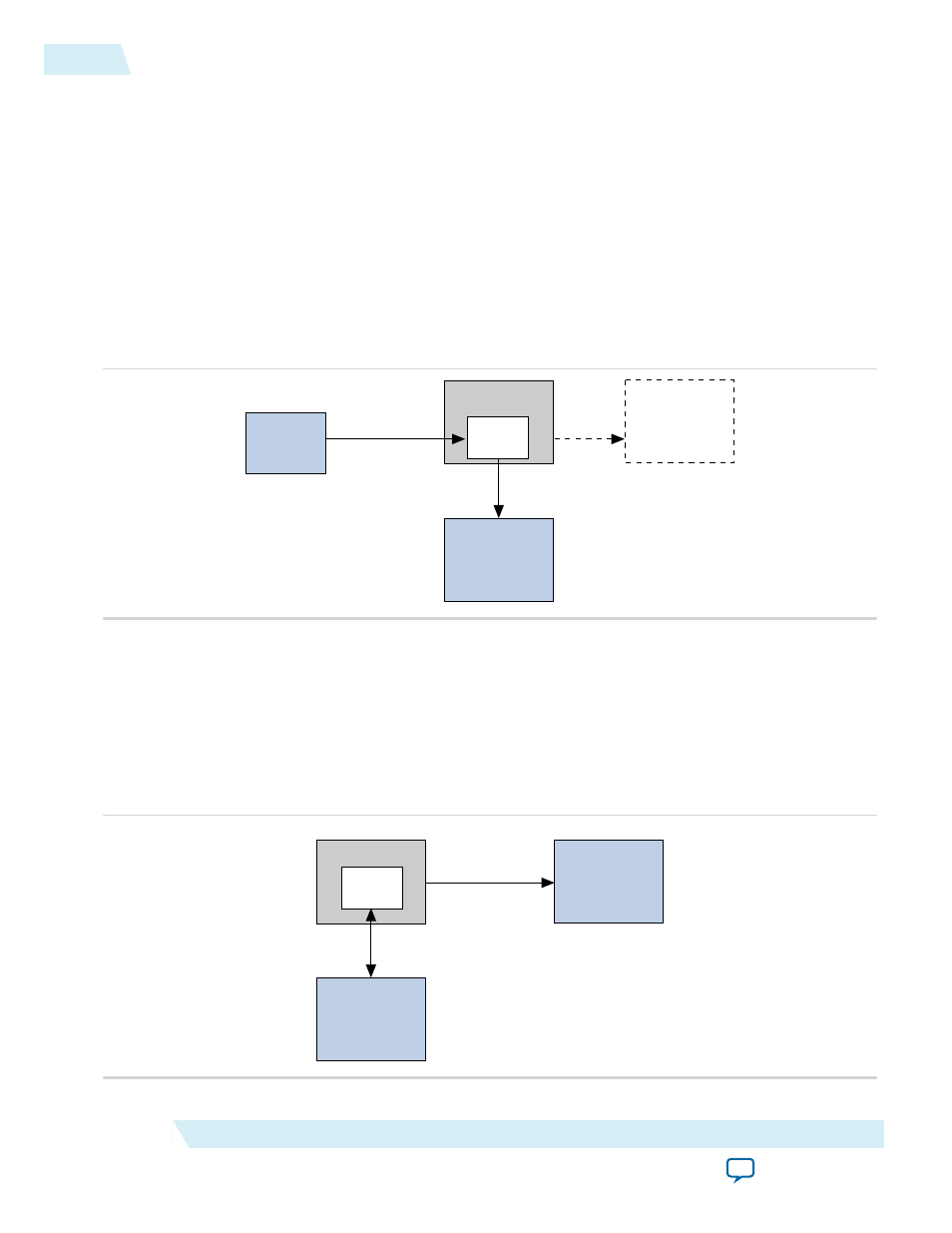
Figure 7: Programming NAND Flash Memory Devices With the JTAG Interface
Figure shows an Altera CPLD functioning as a bridge to program the NAND flash memory device
through the JTAG interface.
Altera CPLD
NAND Flash
Memory
Altera
FPGA
Configuration Data
Open NAND
Flash
Interface
PFL
Quartus II
Software
using JTAG
Altera FPGA Not Used
for Flash Programming
Controlling Altera FPGA Configuration from Flash Memory
You can use the PFL logic in Altera CPLDs as a configuration controller for FPGA configuration. The PFL
logic in the CPLD determines when to start the configuration process, read the data from the flash
memory device, and configure the Altera FPGA in PS or FPP configuration scheme.
Figure 8: FPGA Configuration With Flash Memory Data
Figure shows the Altera CPLD as the configuration controller for the FPGA. The flash memory includes
CFI, quad SPI and NAND flash.
Altera CPLD
Flash
Memory
Altera
FPGA
Flash
Interface
PFL
Passive Serial or
Fast Passive Parallel
Interface
12
Programming NAND Flash
UG-01082
2015.01.23
Altera Corporation
Parallel Flash Loader IP Core User Guide