Programming altera cplds and flash memory devices – Altera Parallel Flash Loader IP User Manual
Page 32
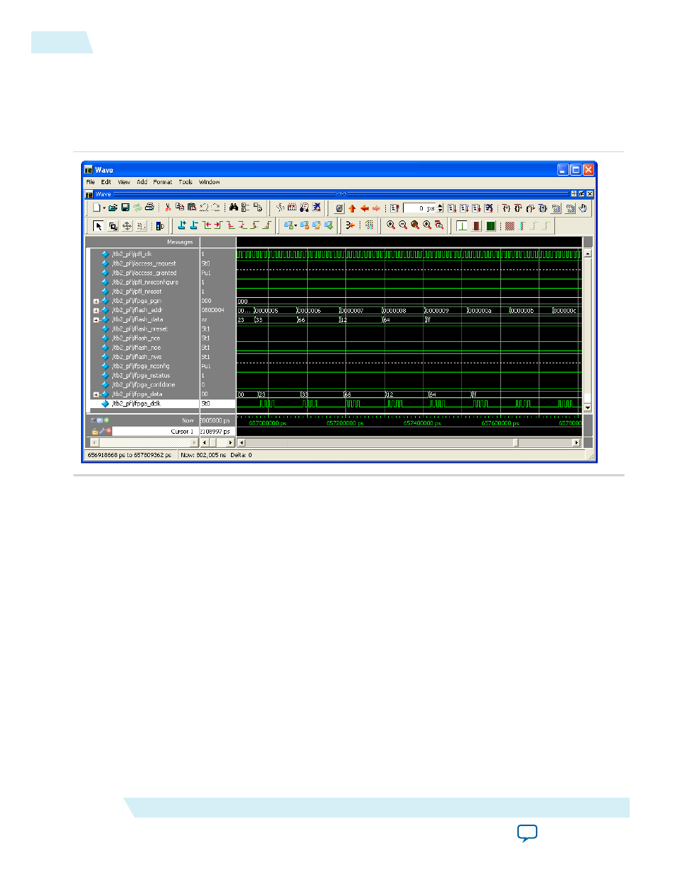
After reading the option bits for page 0, the PFL IP core waits for a period of time before the configuration
starts. The
flash_data
remains at 0×ZZ within this period. Configuration starts when the
fpga_dclk
starts to toggle. During configuration, the PFL IP core asserts the
flash_nce
and
flash_noe
signals low,
and the
pfl_flash_access_request
signal high.
Figure 22: Simulation When FPGA Configuration Starts
The FPGA configuration continues until the
fpga_conf_done
signal is asserted high, which indicates the
configuration is complete. After the configuration process completes, the PFL IP core pulls the
flash_nce
and
flash_noe
signals high and the
pfl_flash_access_request
signal low to indicate the configuration
data is no longer being read from the flash memory device.
Programming Altera CPLDs and Flash Memory Devices
Using the Quartus II Programmer, you can program Altera CPLDs and flash memory device in a single
step or separate steps.
To program both in a single step, first program the CPLD, then the flash memory device. Follow these
steps:
1. Open the Quartus II Programmer window and click Add File to add the
.pof
for the CPLD.
2. Right-click the CPLD
.pof
and click Attach Flash Device.
3. In the Flash Device menu, select the density of the flash memory device to be programmed.
4. Right-click the necessary flash memory device density and click Change File.
32
Programming Altera CPLDs and Flash Memory Devices
UG-01082
2015.01.23
Altera Corporation
Parallel Flash Loader IP Core User Guide