Altera Parallel Flash Loader IP User Manual
Page 36
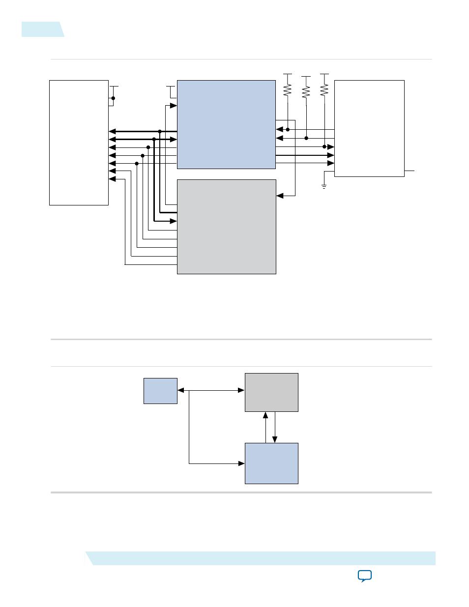
Figure 23: Single-Device Configuration Using the PFL With the Controller
pfl_nreset
pfl_flash_access_granted
flash_addr
flash_data
flash_nwe
flash_nce
flash_noe
pfl_flash_access_request
fpga_conf_done
fpga_nstatus
fpga_nconfig
fpga_data
fpga_dclk
nRP
nWP
ADDR
DATA
nWE
nCE
nOE
WP#/ACC
BYTE#
VCC
10kΩ
VCC
Altera FPGA
Altera CPLD
CFI Flash
10kΩ
VCC
10kΩ
VCC
VCC
(1)
(1)
(1)
(2)
Nios II Processor Interface
(3)
(4)
flash_access_granted
ext_ram_bus_addr
ext_ram_bus_data
write_n_to_ext_flash
chip_n_to_ext_flash
output_n_to_ext_flash
WP#/ACC
BYTE#
flash_access_request
NC
CONF_DONE
nSTATUS
nCONFIG
DATA
DCLK
nCE
nCEO
You must connect the pull-up resistor to a supply that provides an acceptable input signal for the devices. V
CC
must be high enough to meet the V
IH
specification of the I/O
on both devices. For example, the Stratix II V
IH
specification ranges from 1.7 to 3.3 V; therefore, the supply for the pull-up resistor, V
CC
, must be within 1.7 to 3.3 V to meet
the V
IH
specification.
For PS configuration mode, this is a 1-bit data line. For FPP configuration mode, this is an 8-bit data bus.
Do not connect anything to the NC pin (the no connect pin), not even V
CC
or GND.
You can use the Nios II processor in other Altera FPGA, except when you are configuring the FPGA.
(1)
(2)
(3)
(4)
Figure 24: Relationship Between the Four Sections in the Design Example
CFI Flash
Memory
Common Flash
Interface
PFL
pfl_flash_access_granted
pfl_flash_access_request
Altera FPGA
with
NIOS II Processor
Altera CPLD
You must configure the Altera FPGA with the Nios II processor when you power up the board. You can
store the Nios II processor image in the flash memory device and use the PFL IP core to configure the
image to the Altera FPGA. If you store the Nios II processor image in the same flash memory device you
36
PFL IP Core In Embedded Systems
UG-01082
2015.01.23
Altera Corporation
Parallel Flash Loader IP Core User Guide