Altera Parallel Flash Loader IP User Manual
Page 47
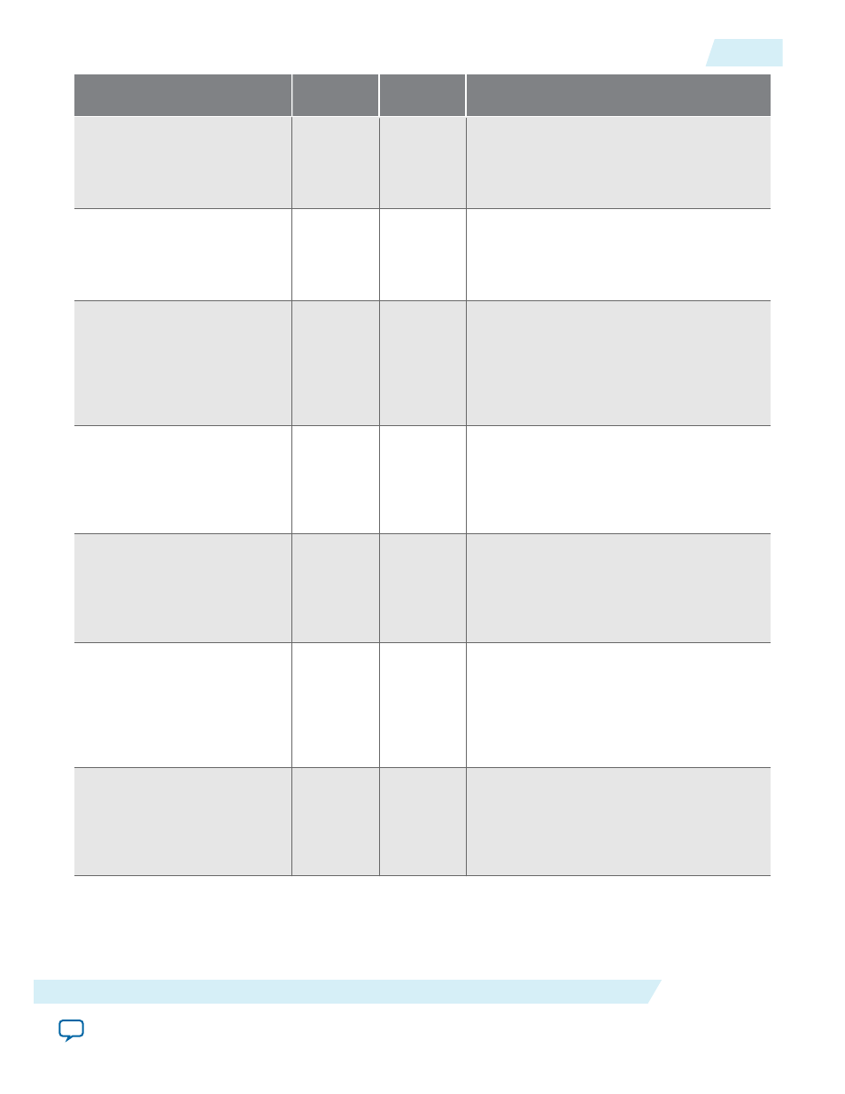
Pin
Description
Weak Pull-
Up
Function
fpga_dclk
Output
—
Connects to the
DCLK
pin of the FPGA.
Clock input data to the FPGA device during
configuration. This pins are not available for
the flash programming option in the PFL IP
core.
fpga_nconfig
Open Drain
Output
10-kW Pull-
Up Resistor
Connects to the
nCONFIG
pin of the FPGA. A
low pulse resets the FPGA and initiates
configuration. This pins are not available for
the flash programming option in the PFL IP
core.
(8)
flash_sck[]
Output
—
Clock source for flash data read operation.
Connects to the
CLK
input pin of the quad
SPI flash. If you use more than one quad SPI
flash, connect this pin to the
CLK
input of all
the quad SPI flashes. The width of the port is
equivalent to the number of quad SPI flash
in the chain.
flash_ncs[]
Output
—
Connects to the ncs pin of the quad SPI
flash. If you use more than one quad SPI
flash, connect this pin to the ncs pin of all
the quad SPI flashes. The width of this port
is equivalent to the number of quad SPI
flashes in the chain.
flash_io0[]
Output
—
The first bit of the data bus to or from the
quad SPI flash. If you use more than one
quad SPI flash, connect this pin to the first
bit of the data bus of all the quad SPI flashes.
The width of this port is equivalent to the
number of quad SPI flashes in the chain.
flash_io1[]
Output
—
The second bit of the data bus to or from the
quad SPI flash. If you use more than one
quad SPI flash, connect this pin to the
second bit of the data bus of all the quad SPI
flashes. The width of this port is equivalent
to the number of quad SPI flashes in the
chain.
flash_io2[]
Output
—
The third bit of the data bus to or from the
quad SPI flash. If you use more than one
quad SPI flash, connect this pin to the third
bit of the data bus of all the quad SPI flashes.
The width of this port is equivalent to the
number of quad SPI flashes in the chain.
UG-01082
2015.01.23
Signals
47
Parallel Flash Loader IP Core User Guide
Altera Corporation