Altera PowerPlay Early Power Estimator User Manual
Page 28
3–12
UG-FPGAPWRCAL-2.0
Altera Corporation
PowerPlay Early Power Estimator User Guide: Stratix, Stratix GX & Cyclone FPGAs
October 2005
PowerPlay Early Power Estimator Input Values
■
M4K blocks
■
M-RAM blocks
Since the power consumption for each type of RAM blocks is different,
the RAM Blocks section in the Stratix or Stratix GX PowerPlay early
power estimator is divided into three parts. Cyclone devices only contain
M4K RAM blocks.
Each row in the RAM Block section represents a design module where
the RAM block(s) have the same frequency, number of data inputs and
outputs, toggle percentage and mode. If some (or all) of the RAM blocks
in your design have different configurations, enter the information in
different rows. For each design module, you need to enter the clock
frequency (f
MAX
) in MHz, the number of data inputs and outputs per
RAM block, the toggle percentage of the data inputs and outputs, the
number of RAM blocks with this configuration, and the mode of each
RAM block.
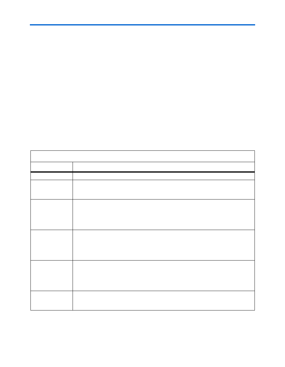
Table 3–5. RAM Blocks Section Information (Part 1 of 2)
Column Heading
Description
Design Module
Enter a name for the design module in this column. This is an optional value.
f
M A X
(MHz)
Enter the frequency of the clock feeding the RAM blocks. If two clocks running at different
frequencies are feeding the RAM block, enter in the higher of the two frequencies. This
value is limited by the maximum frequency specification for each type of RAM block.
# Data Inputs
Enter the number of data inputs per RAM block. If your design consists of many RAM
blocks with different numbers of inputs, you can divide your design into a few design
modules with the same number of inputs. You can find the number of outputs per RAM
block in the timing closure floorplan in the Quartus II software. This value is limited by the
maximum number of inputs available for each type of RAM block.
# Data Outputs
Enter the number of data outputs per RAM block. If your design consists of many RAM
blocks with different numbers of outputs, you can divide your design into a few design
modules with the same number of outputs. You can find the number of outputs per RAM
block in the timing closure floorplan in the Quartus II software. This value is limited by the
maximum number of outputs available for each type of RAM block.
Address Width
Enter the number of address width per RAM block. If your design consists of many RAM
blocks with different numbers of address width, you can divide your design into a few design
modules with the same number of address width. You can find the number of address width
per RAM block in the timing closure floorplan in the Quartus II software. This value is limited
by the maximum number of address width available for each type of RAM block.
Toggle %
Enter the average percentage of RAM data inputs and outputs toggling on each clock cycle.
The toggle percentage ranges from 0 to 100%. Typically, the toggle percentage is 12.5%.
To be more conservative, you can use a higher toggle percentage.