Architecture, Table 2, Multiplexed pin descriptions – Zilog Z80180 User Manual
Page 27
Z8018x
Family MPU User Manual
12
UM005003-0703
ARCHITECTURE
The Z8X180 combines a high performance CPU core with a variety of
system and I/O resources useful in a broad range of applications. The CPU
core consists of five functional blocks: clock generator, bus state controller
(including dynamic memory refresh), interrupt controller, memory
management unit (MMU), and the central processing unit (CPU). The
integrated I/O resources make up the remaining four functional blocks:
•
Direct Memory Access (DMA) Control (2 channels)
•
Asynchronous Serial Communications Interface (ASCI, 2 channels),
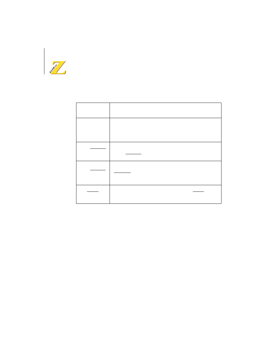
Table 2.
Multiplexed Pin Descriptions
Multiplexed
Pins
Descriptions
A18/TOUT
During RESET, this pin is initialized as A18 pin. If either
TOC1 or TOC0 bit of the Timer Control Register (TCR) is set
to 1, TOUT function is selected. If TOC1 and TOC0 bits are
cleared to 0, A18 function is selected.
CKA0/
DREQ0
During RESET, this pin is initialized as CKA
0
pin.
If either DM1 or SM1 in DMA Mode Register (DMODE) is
set to 1,
DREQ0
function is always selected.
CKA1/
TEND0
During RESET, this pin is initialized as CKA1 pin. If
CKA1D bit in ASCI control register ch 1 (CNTLA1) is set to
1,
TEND0
function is selected. If CKA1D bit is set to 0,
CKA1 function is selected.
RXS/
CTS1
During RESET, this pin is initialized as RXS pin. If CTS1E bit
in ASCI status register ch 1 (STAT1) is set to 1,
CTS1
function
is selected. If CTS1E bit is 0, RXS function is selected.