Figure 11. memory read/write (without wait state), Timing diagram – Zilog Z80180 User Manual
Page 36
Advertising
Z8018x
Family MPU User Manual
UM005003-0703
21
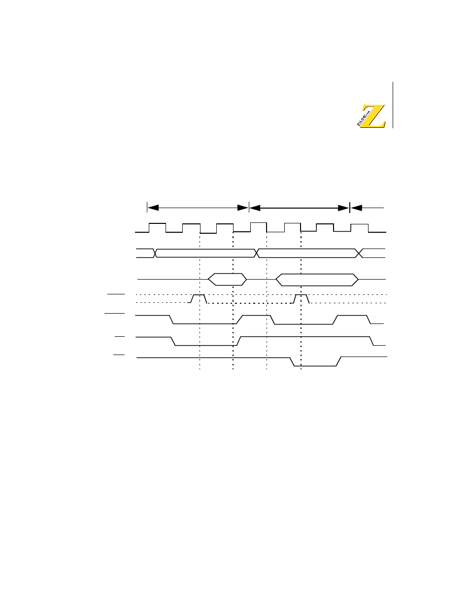
Wait States (TW) are inserted as previously described for Op Code fetch
cycles. Figure 11 illustrates the read/write timing without Wait States
(Tw), while Figure 12 illustrates read/write timing with Wait States (TW).
Figure 11.
Memory Read/Write (without Wait State) Timing Diagram
T1
T1
T2
T3
T1
T2
T3
Phi
A0
–
A19
D0
–
D7
WR
MREQ
RD
WAIT
Read Cycle
Write Cycle
Memory address
Memory address
Write data
Read data
Advertising