Figure 39. int0 mode 2 vector acquisition – Zilog Z80180 User Manual
Page 94
Z8018x
Family MPU User Manual
UM005003-0703
79
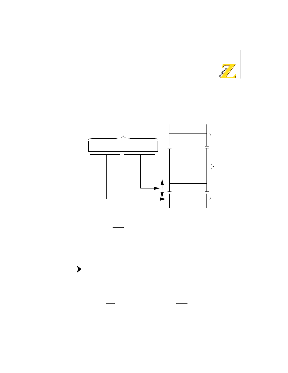
The vector table address is located on 256 byte boundaries in the 64KB
logical address space programmed in the 8-bit Interrupt Vector Register
(1). Figure 39 depicts the INT0 Mode 2 Vector acquisition.
Figure 39. INT0 Mode 2 Vector Acquisition
During the INT0 Mode 2 acknowledge cycle, the low-order 8 bits of the
vector is fetched from the data bus at the rising edge of T3 and the CPU
acquires the 16-bit vector.
Next, the PC is stacked. Finally, the 16-bit restart address is fetched from
the vector table and execution begins at that address.
External vector acquisition is indicated by both MI and IORQ
LOW. Two Wait States (TW) are automatically inserted for
external vector fetch cycles.
During RESET the Interrupt Vector Register (I) is initialized to
00H
and,
if necessary, should be set to a different value prior to the occurrence of a
Mode 2 INT0 interrupt. Figure illustrates INT0 interrupt Mode 2 Timing.
Vector + 1
Vector
Memory
256 Bytes
Vector
Table
16-bit Vector
Offset
Interrupt Vector
Register I
8-bit on
Data Bus
High-order 8 bits
Low-order 8 bits
of starting address
of starting address
Note: