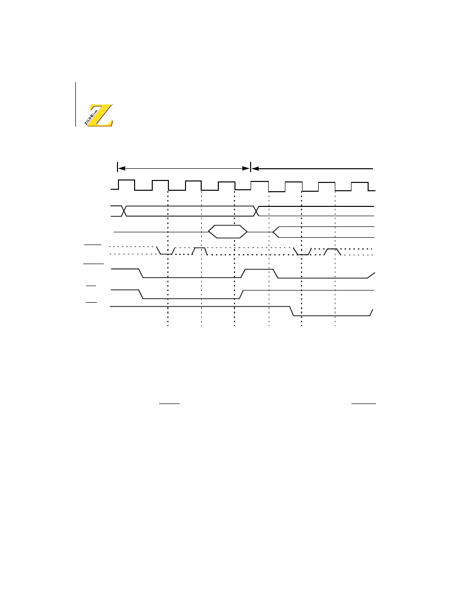
Figure 12. memory read/write (with wait state), Timing diagram – Zilog Z80180 User Manual
Page 37
Advertising
Z8018x
Family MPU User Manual
22
UM005003-0703
Figure 12. Memory Read/Write (with Wait State) Timing Diagram
I/O Read/Write Timing
I/O Read/Write operations differ from memory Read/Write operations in
the following three ways:
•
The IORQ (I/O Request) signal is asserted Low instead of the MREQ
signal
•
The 16-bit I/O address is not translated by the MMU
•
A16–A19 are held Low
At least one Wait State (TW) is always inserted for I/O read and write
cycles (except internal I/O cycles).
Figure 13 illustrates I/O read/write timing with the automatically inserted
Wait State (TW).
T1
T1
T2
TW
T3
T2
T3
Phi
A0
–
A19
D0
–
D7
WR
MREQ
RD
WAIT
Read Cycle
Write Cycle
TW
Read data
Write data
Advertising