Configuration flash memory total programming time, In-system programming – Altera MAX 10 FPGA User Manual
Page 8
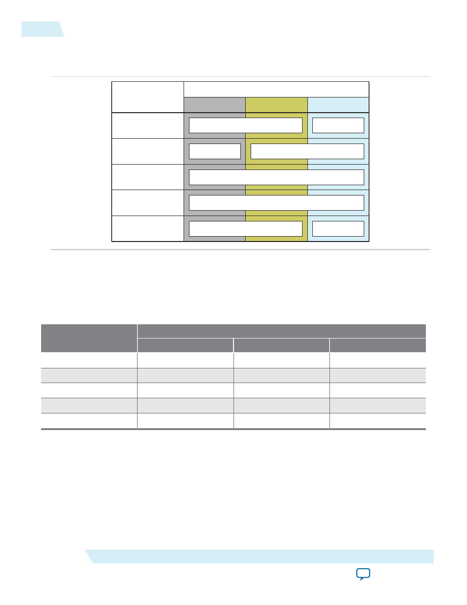
Figure 2-2: Configuration Flash Memory Sectors Utilization for all MAX 10 Devices Except for the
10M02 Device
Unutilized CFM1 and CFM2 sectors can be used for additional user flash memory (UFM).
Configuration Flash Memory Sectors
CFM0
CFM1
CFM2
Dual Compressed Image
Single Uncompressed Image
Single Uncompressed Image
with Memory Initialization
Single Compressed Image
with Memory Initialization
Single Compressed Image
Compressed Image 0
Uncompressed Image 0 with Memory Initialization
Compressed Image 0 with Memory Initialization
Compressed Image 0
Uncompressed Image 0
Compressed Image 1
User Flash Memory
User Flash Memory
Internal Configuration
Mode
Related Information
Configuration Flash Memory Total Programming Time
Table 2-3: Configuration Flash Memory Total Programming Time for Sectors in MAX 10 Devices
Device
Programming Time (s)
CFM2
CFM1
CFM0
10M02
—
—
5.4
10M04
6.5
4.6
11.1
10M08
12.0
8.9
20.8
10M16 and 10M25
16.4
12.6
29.0
10M40 and 10M50
30.2
22.7
52.9
In-System Programming
You can program the internal flash including the CFM of MAX 10 devices with ISP through industry
standard JTAG interface. ISP offers the capability to program, erase, and verify the CFM. The JTAG
circuitry and ISP instructions for MAX 10 devices are compliant to the IEEE-1532-2002 programming
specification.
During ISP, the MAX 10 receives the IEEE Std. 1532 instructions, addresses, and data through the
TDI
input pin. Data is shifted out through the
TDO
output pin and compared with the expected data.
2-4
Configuration Flash Memory Total Programming Time
UG-M10CONFIG
2015.05.04
Altera Corporation
MAX 10 FPGA Configuration Schemes and Features