Altera Phase-Locked Loop Reconfiguration IP Core User Manual
Page 31
Design Example
Page 31
Phase-Locked Loop Reconfiguration (ALTPLL_RECONFIG) Megafunction
February 2012
Altera Corporation
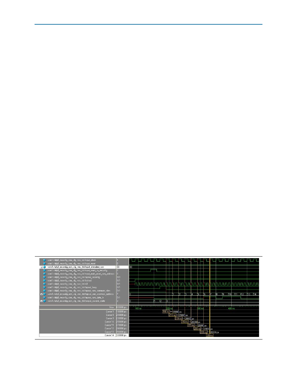
At 170 ns, the state machine is at
2
(indicated by the
output_current_state
signal). At
this state, the state machine is waiting for the assertion of the
tapout_busy
signal,
which signifies the busy signal of the ALTPLL_RECONFIG instantiation. The state
machine tracks the busy signal because whatever operation the ALTPLL_RECONFIG
is in (for example,
read_param
,
write_param
,
reconfig
, or
write_from_rom
) when
asserted for 1 clock cycle, the busy signal is asserted for a particular duration. This
indicates that the particular operation is being processed by the ALTPLL_RECONFIG
instantiation. In this state, the
tapout_busy
signal has been asserted, signifying that
the ALTPLL_RECONFIG instantiation has begun processing the
write_from_rom
operation.
At 190 ns, the state machine is at
3
(indicated by the
output_current_state
signal).
This signifies that the
tapout_busy
signal has been asserted. At this point the state
machine waits until the
tapout_busy
signal gets deasserted, to signify that the process
of writing from the ROM to the scan cache of the ALTPLL_RECONFIG instantiation
has been completed. Observe that the t
apout_rom_common_rden
signal has been
asserted. This is the probed-out signal of the
write_rom_ena
signal, which is part of
the ALTPLL_RECONFIG instantiation. This signal functions as the enable signal to
the ROMs used in this design. Observe that the
tapout_rom_common_address [7:0]
signal begins changing value. This is the probed-out signal of the
rom_address_out
[7:0]
, which is part of the ALTPLL_RECONFIG instantiation. This signal controls
which address of the ROM should be read out to the multiplexer instantiation. When
the
tapout_rom_common_rden
signal is asserted together with the value of 0 for the
tapout_rom_common_address [7:0]
signal, it reads out the data from address 0 of the
ROM 1 to the
q
port of the ROM, which is connected to the
data_0
signal of the
multiplexer. Then the data is multiplexed according to the selector of the multiplexer,
and sent out to the
rom_data_in
port of the ALTPLL_RECONFIG instantiation. This
port is probed out and is observed by the
tapout_rom_data_in
port. Therefore, the
data from the intended ROM can be observed in simulation.
1
The
tapout_rom_common_rden
signal is asserted 1 clock cycle later, after the
tapout_busy
signal is asserted.
shows the simulation results when writing from ROM 1 to the scan cache of
the ALTPLL_RECONFIG megafunction for the duration of 60 to 580 ns.
Figure 25. Initial Writing from ROM 1 to the Scan Cache of the ALTPLL_RECONFIG Megafunction (60 to 580 ns)