Altera Phase-Locked Loop Reconfiguration IP Core User Manual
Page 8
Page 8
Functional Description—Implementing Multiple Reconfiguration Using an External ROM
Phase-Locked Loop Reconfiguration (ALTPLL_RECONFIG) Megafunction
February 2012
Altera Corporation
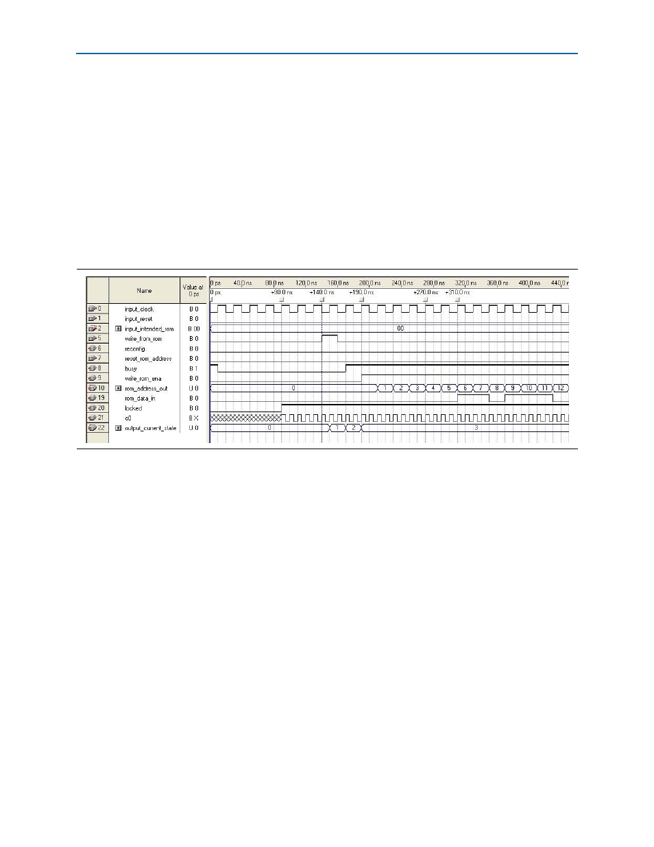
To copy the data from a ROM to the ALTPLL_RECONFIG megafunction scan cache (a
memory location that stores the PLL reconfiguration settings), you must hold the
write
_
from
_
rom
signal high for 1 clock cycle. The megafunction asserts the busy
signal on the first rising edge of the clock after the
write
_
from
_
rom
signal goes high.
The busy signal remains asserted until all the bits are written into the scan cache.
On the second rising edge of the clock after the
write
_
from
_
rom
signal goes low
again, the intended ROM address for the write operation appears on the
rom
_
address
_
out
port. The data of the ROM specified by the intended address on
rom
_
address
_
out
is fed to the r
om
_
data
_
in
input port of the ALTPLL_RECONFIG
megafunction instantiation. The
write
_
rom
_
ena
signal is also asserted on the second
rising edge of the clock after the
write
_
from
_
rom
signal goes low again (refer to
The writing-to-scan cache process continues until the address reaches the specific size
of the scan cache (234 for Stratix III device top and bottom PLL, 180 for Stratix III
device left and right PLL, and 144 for Cyclone III PLL). This process is completed
when the
busy
signal is deasserted. This means that the scan cache of the
ALTPLL_RECONFIG megafunction is written with the intended reconfiguration
settings from the ROM.
Figure 5. Beginning Write to the Scan Cache of the ALTPLL_RECONFIG Megafunction from the ROM