Altera Phase-Locked Loop Reconfiguration IP Core User Manual
Page 32
Page 32
Design Example
Phase-Locked Loop Reconfiguration (ALTPLL_RECONFIG) Megafunction
February 2012
Altera Corporation
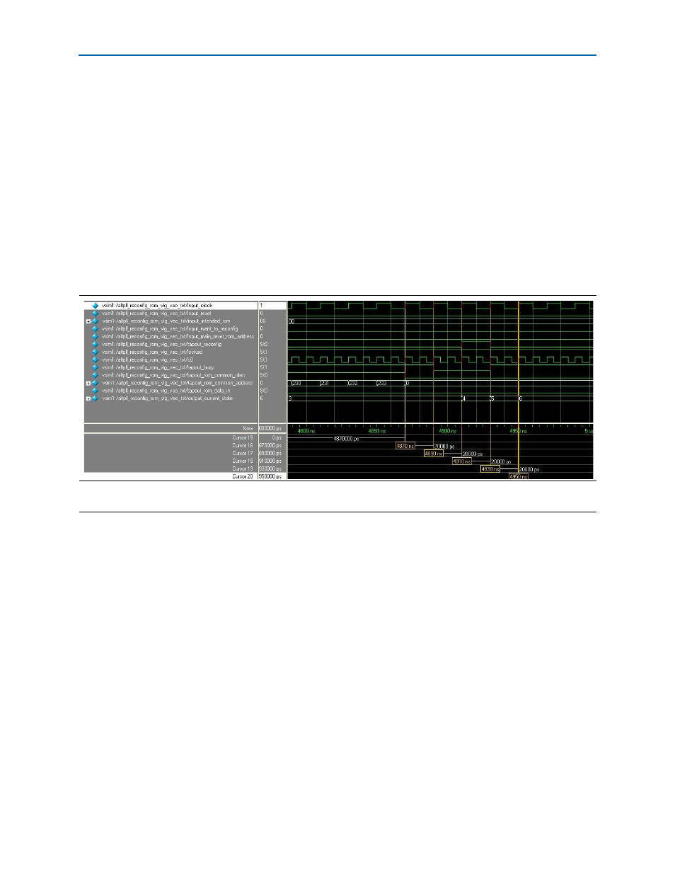
When data from the ROM is written to the scan cache of the ALTPLL_RECONFIG, it
is done serially, meaning a 1-by-1 bit per cycle, from address
0
to address 233. You can
observe this via the
tapout_rom_data_in
signal. The valid data read out from the
ROM is delayed by 2 clock cycles.
When the simulation is at 270 ns, the
tapout_rom_common_rden
signal is asserted with
the
tapout_rom_common_address [7:0]
signal with a value of 4. The data read out has
a value of 1 in the
.mif file in
. However, this value only appears when the
tapout_rom_common_rden
signal is asserted via the
tapout_rom_common_address
[7:0]
signal with a value of 6 at 310 ns, implying a 2-clock-cycle delay.
This writing process continues until it has reached address
233
shows the
simulation results of the final process in writing the contents of ROM 1 to the scan
cache of the ALTPLL_RECONFIG megafunction.
At 4850 ns, the
tapout_rom_common_rden
signal is asserted with the
tapout_rom_common_address [7:0]
signal with a value of 233. This is the last address
read out from ROM 1.
1
The data is available only 2 clock cycles later on the
tapout_rom_data_in
signal. The
tapout_rom_common_rden
signal and the
tapout_busy
signal are still asserted. The
output_current_state
signal still has a value of 3. It will remain in this state until the
tapout_busy
signal is deasserted.
At 4870 ns, the
tapout_rom_common_rden
signal is deasserted with the
tapout_rom_common_address [7:0]
signal with a value of 0. This stops the ROM 1
from reading out data; therefore, the address becomes 0. The
tapout_rom_data_in
signal still generates valid output data and the
tapout_busy
signal is asserted. The
output_current_state
signal still has a value of
3.
At 4890 ns, the
tapout_rom_common_rden
signal remains deasserted with the
tapout_rom_common_address [7:0]
signal with a value of
0
. Observe that the
tapout_rom_data_in
signal generates the last valid output data from ROM 1 (from
address 233). The
tapout_busy
signal is deasserted and the
output_current_state
signal still has a value of
3
.
Figure 26. Ending Process of Writing the Contents of ROM 1 to the Scan Cache of the ALTPLL_RECONFIG Megafunction
(4700 to 5040 ns)
Note to
(1) This figure also shows the initialization of the reconfiguration process.