Specifications, Verilog hdl prototype – Altera Phase-Locked Loop Reconfiguration IP Core User Manual
Page 37
Specifications
Page 37
Phase-Locked Loop Reconfiguration (ALTPLL_RECONFIG) Megafunction
February 2012
Altera Corporation
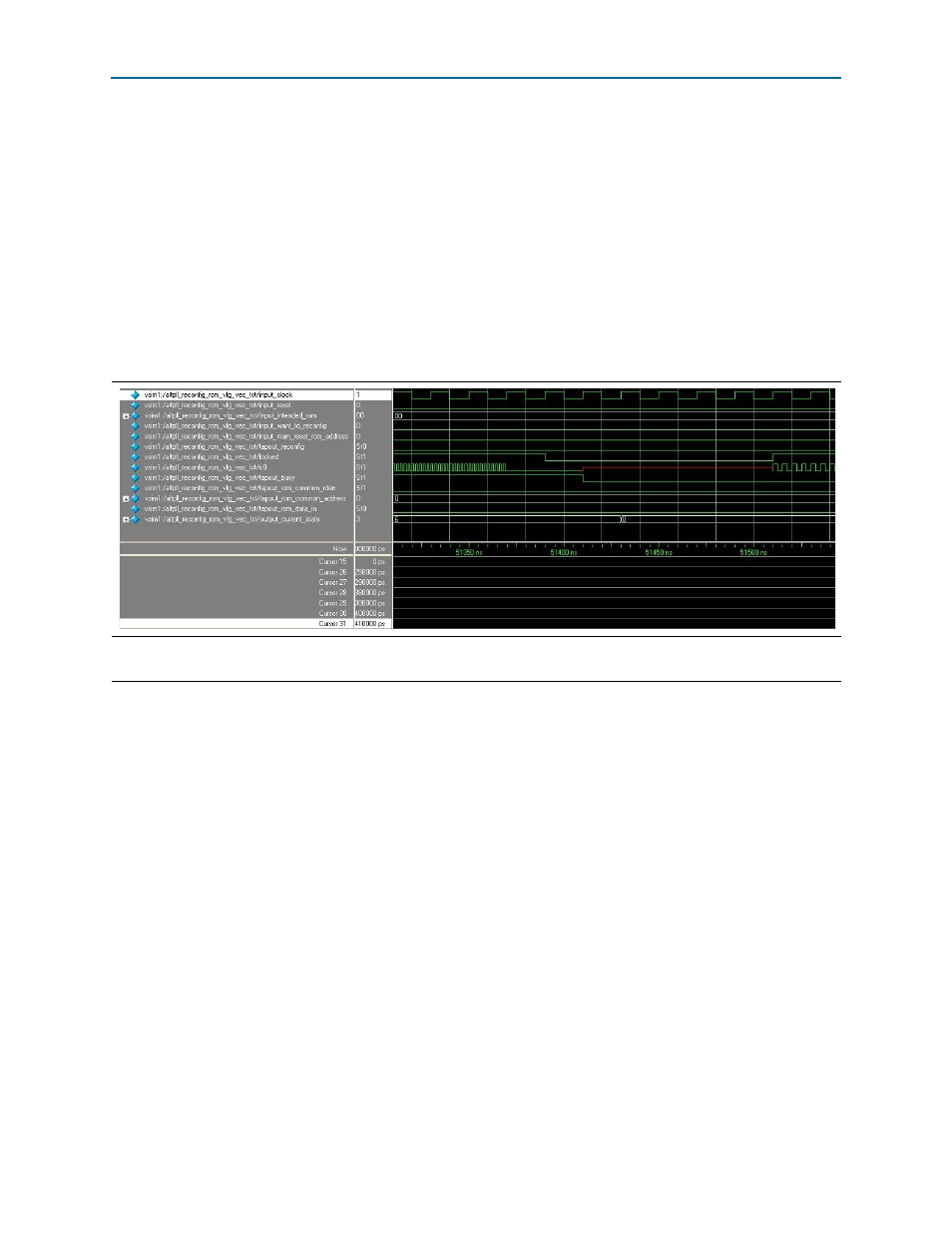
At 41,390 ns, the
tapout_rom_common_rden
signal is deasserted for 1 clock cycle. The
tapout_rom_common_address [7:0]
signal is changed to a value of
0
. The
tapout_rom_data_in
signal still generates the previous 2-clock-cycle output data
(address 9), which is of value 1. The
tapout_busy
signal is still asserted. The
output_current_state
signal is
3
.
At 41,410 ns, the
tapout_rom_common_rden
signal is reasserted. The
tapout_rom_common_address [7:0]
signal is changed to a value of
0
. This restarts the
writing of the contents of ROM 1 to the ALTPLL_RECONFIG scan cache from address
0. The
tapout_busy
signal is still asserted. The
output_current_state
signal is
3
.
The PLL reconfiguration process continues as normal until the
c0
signal is 200 MHz,
You can modify the design to suit your requirements when attempting to reconfigure
the PLL from multiple .mif files via external ROMs.
Specifications
This section describes the prototypes, component declarations, ports, and parameters
of the ALTPLL_RECONFIG megafunction. These ports and parameters are available
to customize the ALTPLL_RECONFIG megafunction according to your application.
Verilog HDL Prototype
The following Verilog HDL prototype is located in the Verilog Design File (.v)
altera_mf.v
in the <Quartus II installation directory>\eda\synthesis directory.
modulealtpll_reconfig
#(
parameterintended_device_family = "unused",
parameterinit_from_rom = "NO",
parameterpll_type = "UNUSED",
parameterscan_chain = "UNUSED",
parameterscan_init_file = "UNUSED",
Figure 33. PLL Reconfiguration From ROM1 (40,800 to 41,090 ns)
Note to
(1) From
c0
= 500 MHz to
c0
= 200 MHz.