Figure 2–1, Table 2–1 – Altera Cyclone III LS FPGA Development Board User Manual
Page 10
2–2
Chapter 2: Board Components
Board Overview
Cyclone III LS FPGA Development Board Reference Manual
© October 2009 Altera
Corporation
describes the components and lists their corresponding board references.
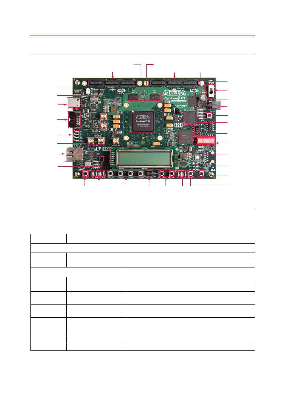
Figure 2–1. Overview of the Cyclone III LS FPGA Development Board Features
Clock Input SMAs
Connector (J7, J9)
Max II Reset
Push-Button
Switch (S10)
General User
Push-buttons
Switches
(S3 - S6)
Board Settings
DIP Switch (SW2)
DC Input Jack (J5)
Cyclone III LS FPGA (U15)
Character LCD
(J19)
CPU Reset
Push-button
Switch (S2)
Power Switch (SW1)
General
User DIP
Switch (S7)
General
User LEDs
(D25-D28)
MAX II CPLD
EPM2210 System
Controller (U22)
Clock Output SMA
Connector (J15)
HSMC Port B (J1)
HSMC Port A (J2)
Configuration Status
LEDs (D10-D14)
Flash x16 Memory (U9)
DDR2 Memory (U5, U6)
Programmable
Oscillator Output
(J13, J14)
USB Type-B
Connector (J4)
Gigabit Ethernet
Port (J16)
JTAG Connector
(J8)
SSRAM x36
Memory (U14)
Configuration
Select
LEDs
(D29-D31)
Configuration
Program and
Select
Push-buttons
Switches (S8, S9)
Power LED (D3)
JTAG Chain Header
& JTAG Select
Jumpers (J11, J12)
CRC Error (S1)
JTAG Anti-Tamper
Select LEDs (D6-D9)
LCD/HSMC Port B
Data Select (J18)
VCCA Shutdown
Push-Button
Switch (S11)
Table 2–1. Cyclone III LS FPGA Development Board Components (Part 1 of 3)
Board Reference
Type
Description
Featured Devices
U15
FPGA
EP3CLS200F780, 780-pin FBGA.
U22
CPLD
EPM2210F256, 256-pin FBGA.
Configuration, Status, and Setup Elements
J4
USB type-B connector
Connects to the computer to enable embedded USB-Blaster JTAG.
J11
JTAG chain header
Enables and disables devices in the JTAG chain.
J12
Anti-Tamper JTAG select
header
Placing a shunt on this jumper breaks the default JTAG chain, giving
FPGA JTAG signals control to the MAX II EPM2210 System Controller.
D6
Anti-Tamper JTAG select LED
Illuminated when the default JTAG chain is broken and the MAX II
EPM2210 System Controller has control of the FPGA JTAG signals.
SW2
Board settings DIP switch
Controls the MAX
II CPLD EPM2210 System Controller functions such
as clock enable, SMA clock input control, and which image to load
from flash memory at power-up.
J8
JTAG connector
Disables embedded blaster (for use with external USB-Blasters).
D13
Configuration done LED
Illuminates when the FPGA is configured.