Development board block diagram, Handling the board – Altera Cyclone III LS FPGA Development Board User Manual
Page 8
1–4
Chapter 1: Overview
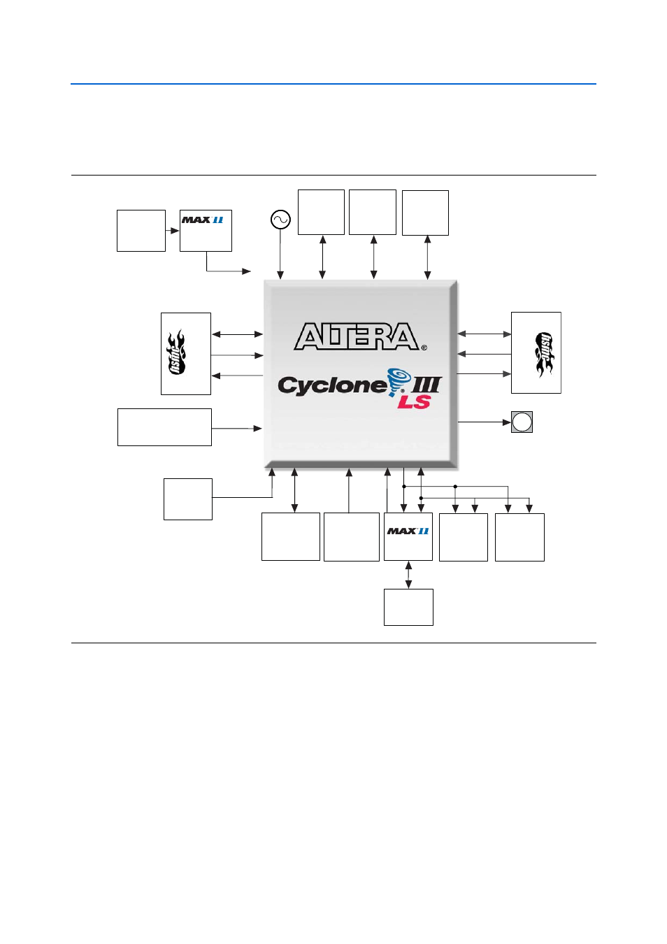
Development Board Block Diagram
Cyclone III LS FPGA Development Board Reference Manual
© October 2009 Altera Corporation
Development Board Block Diagram
shows the block diagram of the Cyclone III LS FPGA development board.
Handling the Board
When handling the board, it is important to observe the following static discharge
precaution:
c
Without proper anti-static handling, the board can be damaged. Therefore, use
anti-static handling precautions when touching the board.
Figure 1–1. Cyclone III LS FPGA Development Board Block Diagram
EP3CLS200F780
Port B
Port A
EEPROM
(32 Kbit I
2
C)
2x16 LCD
Push-button
Switches,
DIP Switches,
LEDs
CPLD
64 Mbyte
Flash
2 Mbyte
SSRAM
512 Mbyte
DDR2 (x16)
Gigabit
Ethernet
PHY (RGMII)
Clock_SMA
Programmable Oscillator
100 M, 125 M, 156.25 M,
SMA (LVPECL)
Embedded
Blaster
USB
2.0
x47
x16
x2 CLK IN
x2
x11
x13
x26 ADDR
Config I/O
x74
CLKIN x2
CLKOUT x2
x74
CLKIN x3
CLKOUT x3
JTAG Chain
x32 DATA
x1 CLK IN
(1.8 V)
Migratable to
EP3CLS70F780
Z
Z
66.6 MHz
512 Mbyte
DDR2 (x16)
x47
SMA
Anti-Tamper
Example
Design
x6
(LVPECL)