Altera Cyclone III LS FPGA Development Board User Manual
Page 23
Chapter 2: Board Components
2–15
Configuration, Status, and Setup Elements
© October 2009 Altera Corporation
Cyclone III LS FPGA Development Board Reference Manual
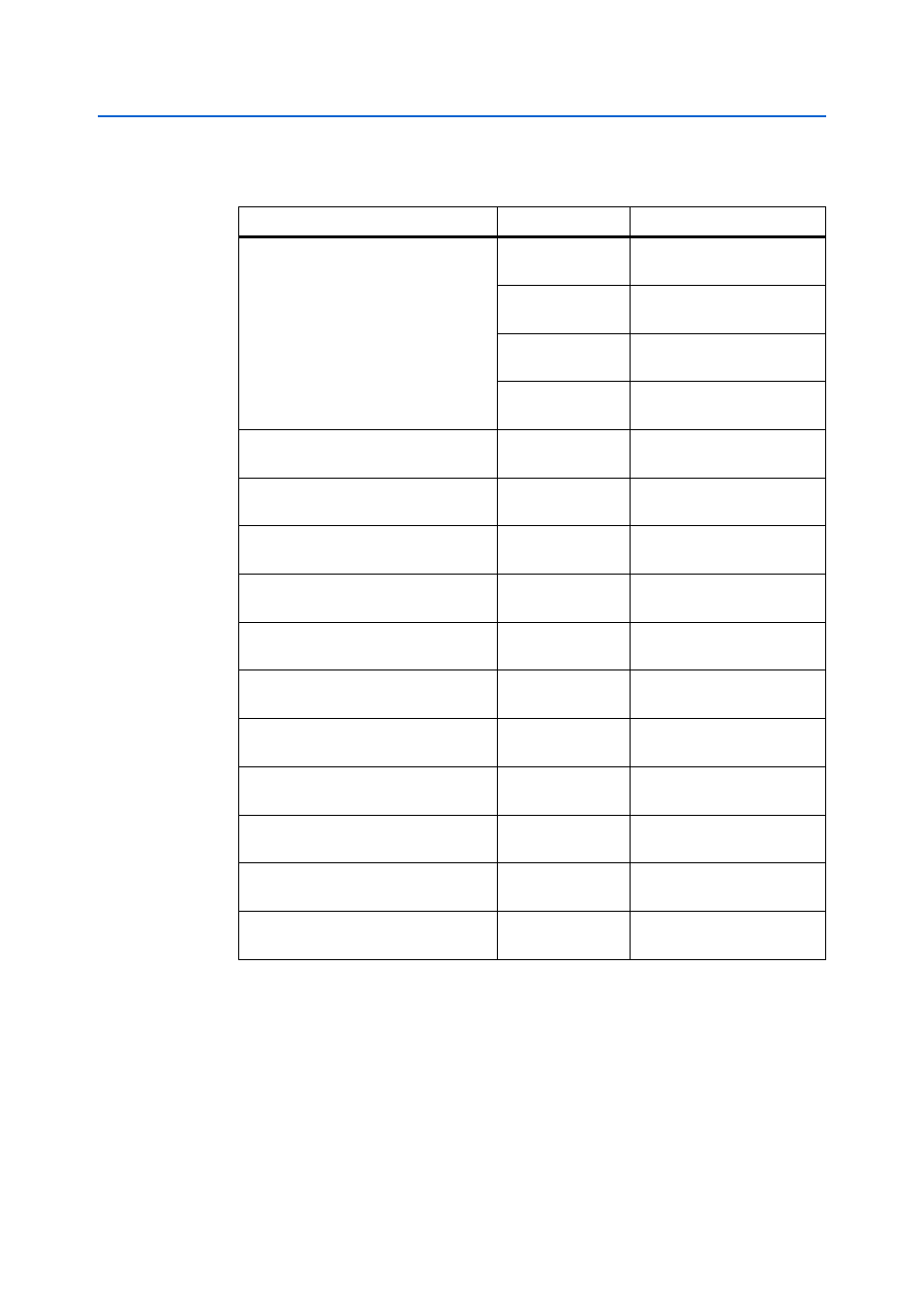
shows the flash memory map storage.
There are two pages reserved for the FPGA configuration data. The factory hardware
page is considered page 0 and is loaded upon power-up if the USER_PGM DIP switch
(SW2.6) is set to '0'. Otherwise, the user hardware page 1 is loaded. Pressing the PGM
configure push-button switch (S8) loads the FPGA with a hardware page based on
which PGM_LED[2:0] (D29, D30, D31) LED is illuminated.
defines the
hardware page that loads when the PGM configure push-button switch (S8) is
pressed.
Table 2–7. Flash Memory Map
Name
Size
Address
Unused
32 KB
0x03FF-FFFF
0x03FF-8000
32 KB
0x03FF-7FFF
0x03FF-0000
32 KB
0x03FE-FFFF
0x03FE-8000
32 KB
0x03FE-7FFF
0x03FE-0000
User software
24,320 KB
0x03FD-FFFF
0x0282-0000
Factory software
8,192 KB
0x0281-FFFF
0x0202-0000
zipfs — HTML, web content
8,192 KB
0x0201-FFFF
0x0182-0000
Unused
6,095 KB
0x0181-FFFF
0x0128-0000
User hardware 2
6,357 KB
0x0127-FFFF
0x00C6-0000
User hardware 1
6,357 KB
0x00C5-FFFF
0x0064-0000
Factory hardware
6,357 KB
0x0063-FFFF
0x0002-0000
PFL option bits
32 KB
0x0001-FFFF
0x0001-8000
Reserved
32 KB
0x0001-7FFF
0x0001-0000
Ethernet option bits (MAC address)
32 KB
0x0000-FFFF
0x0000-8000
User design reset vector
32 KB
0x0000-7FFF
0x0000-0000