High-speed mezzanine cards, High-speed mezzanine cards –29 – Altera Cyclone III LS FPGA Development Board User Manual
Page 37
Chapter 2: Board Components
2–29
Components and Interfaces
© October 2009 Altera Corporation
Cyclone III LS FPGA Development Board Reference Manual
High-Speed Mezzanine Cards
The development board contains two HSMC interfaces called port A and port B.
HSMC port A interface supports both single-ended and differential signaling while
HSMC port B interface only supports single-ended signaling. The HSMC interface
also allows JTAG, SMB, clock outputs and inputs, as well as power for compatible
HSMC cards. The HSMC is an Altera-developed open specification, which allows you
to expand the functionality of the development board through the addition of
daughtercards (HSMCs).
f
For more information about the HSMC specification such as signaling standards,
signal integrity, compatible connectors, and mechanical information, refer to the
manual.
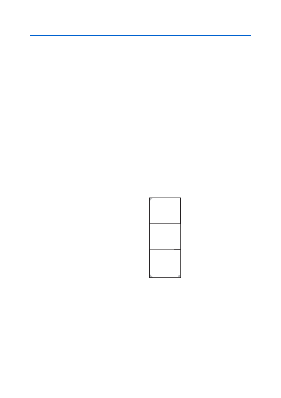
The HSMC connector has a total of 172 pins, including 120 signal pins, 39 power pins,
and 13 ground pins. The ground pins are located between the two rows of signal and
power pins, acting both as a shield and a reference. The HSMC host connector is
based on the 0.5 mm-pitch QSH/QTH family of high-speed, board-to-board
connectors from Samtec. There are three banks in this connector. Bank 1 has every
third pin removed as done in the QSH-DP/QTH-DP series. Bank 2 and bank 3 have
all the pins populated as done in the QSH/QTH series.
shows the bank arrangement of signals with respect to the Samtec
connector's three banks.
The HSMC interface has programmable bi-directional I/O pins that can be used as
2.5-V LVCMOS, which is 3.3-V LVTTL-compatible. These pins can also be used as
various differential I/O standards including, but not limited to, LVDS, mini-LVDS,
and RSDS with up to 17 full-duplex channels.
1
As noted in the
manual, LVDS and
single-ended I/O standards are only guaranteed to function when mixed according to
either the generic single-ended pin-out or generic differential pin-out.
Figure 2–9. HSMC Signal and Bank Diagram
Bank 3
Power
D(79.40)
-or-
LVDS
CLKIN2, CLKOUT2
Bank 2
Power
D(39:0)
-or-
D[3:0] + LVDS
CLKIN1, CLKOUT1
Bank 1
8 TX Channels CDR
8 RX Channels CDR
JTAG
SMB
CLKIN0, CLKOUT0