Featured device: cyclone iii ls device, Featured device: cyclone iii ls device –4 – Altera Cyclone III LS FPGA Development Board User Manual
Page 12
2–4
Chapter 2: Board Components
Featured Device: Cyclone III LS Device
Cyclone III LS FPGA Development Board Reference Manual
© October 2009 Altera
Corporation
Featured Device: Cyclone III LS Device
The Cyclone III LS FPGA development board features the Cyclone III LS
EP3CLS200F780 device (U15) in a 780-pin FBGA package.
f
For more information about Cyclone III device family, re
describes the features of the Cyclone III LS EP3CLS200F780 device.
lists the Cyclone III LS device component reference and manufacturing
information.
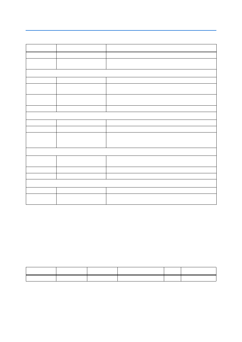
S3, S4, S5, S6
User push-button switches
Four user push-button switches. Driven low when pressed.
J19
Character LCD
Connector which interfaces to the provided 16 character × 2 line LCD
module.
Memory Devices
U5, U6
DDR2 x16 memory
Two independent 16-bit, 64-Mbyte DDR2 devices.
U14
SSRAM x36 memory
Standard synchronous RAM which makes a 36-bit 2-Mbyte SSRAM
port.
U9
Flash x16 memory
Synchronous burst mode flash device which provides a 16-bit 64-
Mbyte non-volatile memory port.
U21
EEPROM
I
2
C EEPROM
Components and Interfaces
J2
HSMC port A
Provides 80 CMOS or 17 LVDS channels per the HSMC specification.
J1
HSMC port B
Provides 76 CMOS channels per the HSMC specification.
J16
Gigabit Ethernet
RJ-45 connector which provides a 10/100/1000 Ethernet connection
via a Marvell 88E1111 PHY and the FPGA-based Altera Triple Speed
Ethernet MegaCore function in RGMII mode.
Anti-Tamper Interface
J10
JTAG header to MAX II general
I/O
JTAG header connected to general purpose I/O (GPIO) on the MAX II
EPM2210 System Controller.
D8, D9, D10
Anti-Tamper status LEDs
Three anti-tamper status indicator LEDs.
S1
CRC error push-button
Insert a CRC error when running the anti-tamper example design.
Power Supply
J5
DC input jack
Accepts a 14-V – 20-V DC power supply.
SW1
Power switch
Switch to power on or off the board when power is supplied from the
DC input jack.
Table 2–1. Cyclone III LS FPGA Development Board Components (Part 3 of 3)
Board Reference
Type
Description
Table 2–2. Cyclone III LS Device EP3CLS200F780 Features
Equivalent LEs
M9K RAM Blocks
Total RAM Kbits
18-bit × 18-bit Multipliers
PLLs
Package Type
198,464
891
8,211
396
4
780-pin FBGA