General user input/output, User-defined push-button switches, General user input/output –23 – Altera Cyclone III LS FPGA Development Board User Manual
Page 31: User-defined push-button switches –23
Chapter 2: Board Components
2–23
General User Input/Output
© October 2009 Altera Corporation
Cyclone III LS FPGA Development Board Reference Manual
lists the clock outputs for the Cyclone III LS FPGA development board.
lists the crystal oscillators component references and manufacturing
information.
General User Input/Output
This section describes the user I/O interface to the FPGA, including the push-buttons,
DIP switches, status LEDs, and character LCD.
User-Defined Push-Button Switches
The development board includes five user-defined push-button switches: four general
user push-button switches and one CPU reset. For information on the system and safe
reset push-button switches, refer to
“Configuration Push-button Switches” on
Board references S3 through S6 are push-button switches that allow you to interact
with the Cyclone III LS device. When the switch is pressed and held down, the device
pin is set to logic 0; when the switch is released, the device pin is set to logic 1. There is
no board-specific function for these general user push-button switches.
The board reference S2 is the CPU reset push-button switch, CPU_RESETn, which is
an input to the Cyclone III LS device and the MAX II CPLD EPM2210 System
Controller. CPU_RESETn is intended to be the master reset signal for the FPGA design
loaded into the Cyclone III LS device. This switch also acts as a regular I/O pin.
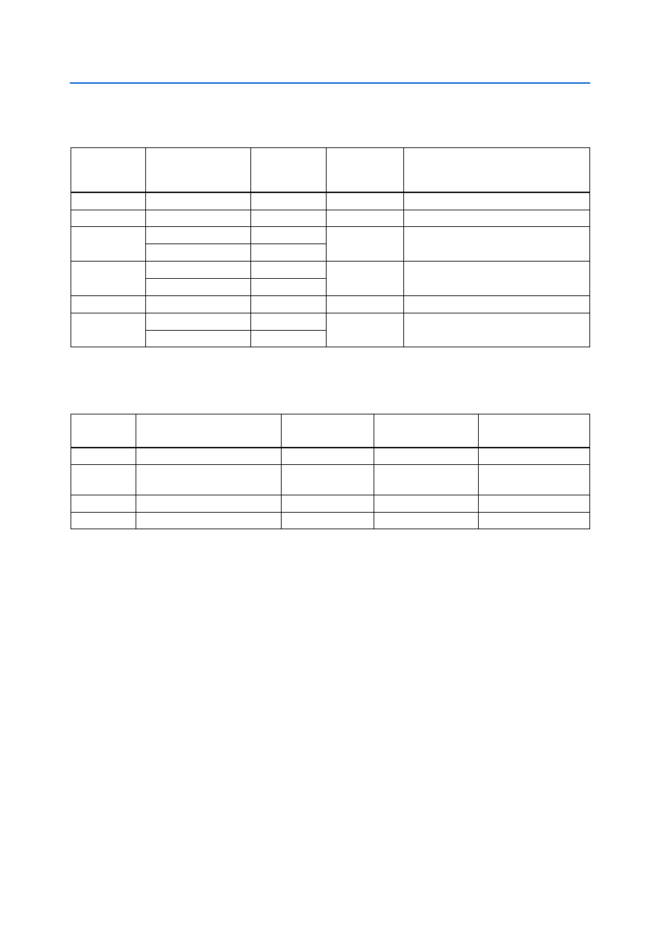
Table 2–21. Cyclone III LS FPGA Development Board Clock Outputs
Connector
Schematic Signal
Name
Cyclone III LS
Device Pin
Number
I/O Standard
Description
SMA (J15)
CLKOUT_SMA
AC15
2.5-V
FPGA CMOS output or GPIO
Samtec HSMC
HSMA_CLKOUT0
P28
2.5-V
FPGA CMOS output or GPIO
Samtec HSMC
HSMA_CLKOUT_P1
V28
LVDS or 2.5-V
LVDS output or two 2.5-V CMOS outputs.
HSMA_CLKOUT_N1
U28
Samtec HSMC
HSMA_CLKOUT_P2
M25
LVDS or 2.5-V
LVDS output or two 2.5-V CMOS outputs.
HSMA_CLKOUT_N2
N26
Samtec HSMC
HSMB_CLKOUT0
D2
2.5-V
FPGA CMOS output or GPIO
Samtec HSMC
HSMB_CLKOUT_P2
T6
LVDS or 2.5-V
LVDS output or two 2.5-V CMOS outputs.
HSMB_CLKOUT_N2
T5
Table 2–22. Crystal Oscillator Component References and Manufacturing Information
Board
Reference
Description
Manufacturer
Manufacturer
Part Number
Manufacturer Website
X3
66.6 MHz Crystal Oscillator
ECS Inc.
ECS-3953C-666-X
U17
Single Output Programmable
Clock Generator
Texas Instruments
CDCM61001RHB
X5
50.00 MHz Crystal Oscillator
ECS Inc.
ECS-3525-500-B-xx
Y3
100.00 MHz Crystal Oscillator
Pletronics
SM5545TEX-100.00M