Ddr2, Ddr2 –36 – Altera Cyclone III LS FPGA Development Board User Manual
Page 44
2–36
Chapter 2: Board Components
Memory
Cyclone III LS FPGA Development Board Reference Manual
© October 2009 Altera
Corporation
DDR2
There are two DDR2 devices, providing 512 Mbit of memory each for a total of
1024 Mbit of on-board DDR2 SDRAM. Each device interface has a 16-bit data bus,
which can be configured to run individually or together as a 32-bit data bus. One of
the device is pinned out to FPGA bank 7 and a second device is pinned out to FPGA
bank 8. These memory interfaces are designed to run at a maximum fequency of
167 MHz for a maximum theoretical bandwidth of over 10.6 Gbps. The internal bus in
the FPGA is typically 2 or 4 times the width at full rate or half rate respectively. For
example, a 167 MHz 16-bit interface will become a 83.5 MHz 64-bit bus.
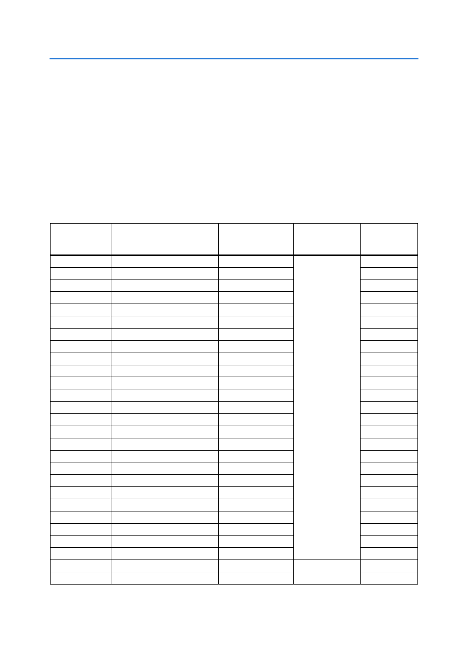
lists the DDR2 bank 7 pin assignments, signal names, and its functions. The
signal names and types are relative to the Cyclone III LS device in terms of I/O setting
and direction.
Table 2–37. DDR2 Bank 7 Pin Assignments, Signal Names and Functions (Part 1 of 2)
Board Reference
Description
Schematic Signal
Name
I/O Standard
Cyclone III LS
Device
Pin Number
U6.M8
Address bus
DDR2_B7_A0
1.8-V SSTL Class I
E19
U6.M3
Address bus
DDR2_B7_A1
C24
U6.M7
Address bus
DDR2_B7_A2
A23
U6.N2
Address bus
DDR2_B7_A3
C15
U6.N8
Address bus
DDR2_B7_A4
D19
U6.N3
Address bus
DDR2_B7_A5
D16
U6.N7
Address bus
DDR2_B7_A6
A22
U6.P2
Address bus
DDR2_B7_A7
A15
U6.P8
Address bus
DDR2_B7_A8
A20
U6.P3
Address bus
DDR2_B7_A9
A17
U6.M2
Address bus
DDR2_B7_A10
C16
U6.P7
Address bus
DDR2_B7_A11
D18
U6.R2
Address bus
DDR2_B7_A12
D15
U6.R8
Address bus
DDR2_B7_A13
D17
U6.R3
Address bus
DDR2_B7_A14
E16
U6.R7
Address bus
DDR2_B7_A15
E17
U6.L2
Bank address bus
DDR2_B7_BA0
F22
U6.L3
Bank address bus
DDR2_B7_BA1
F19
U6.L1
Bank address bus
DDR2_B7_BA2
F16
U6.L7
Column address select
DDR2_B7_CASn
F17
U6.K2
Clock enable
DDR2_B7_CKE
B15
U6.L8
Chip select rank 0
DDR2_B7_CSn
A19
U6.K9
Termination enable rank 0
DDR2_B7_ODT
A18
U6.K7
Row address select
DDR2_B7_RASn
G16
U6.K3
Write enable
DDR2_B7_WEn
B24
U6.J8
Clock P
DDR2_B7_CLK_P
Differential 1.8-V
SSTL Class I
D25
U6.K8
Clock N
DDR2_B7_CLK_N
C25