I/o resources, I/o resources –5, Table 2–3 – Altera Cyclone III LS FPGA Development Board User Manual
Page 13
Chapter 2: Board Components
2–5
Featured Device: Cyclone III LS Device
© October 2009 Altera Corporation
Cyclone III LS FPGA Development Board Reference Manual
I/O Resources
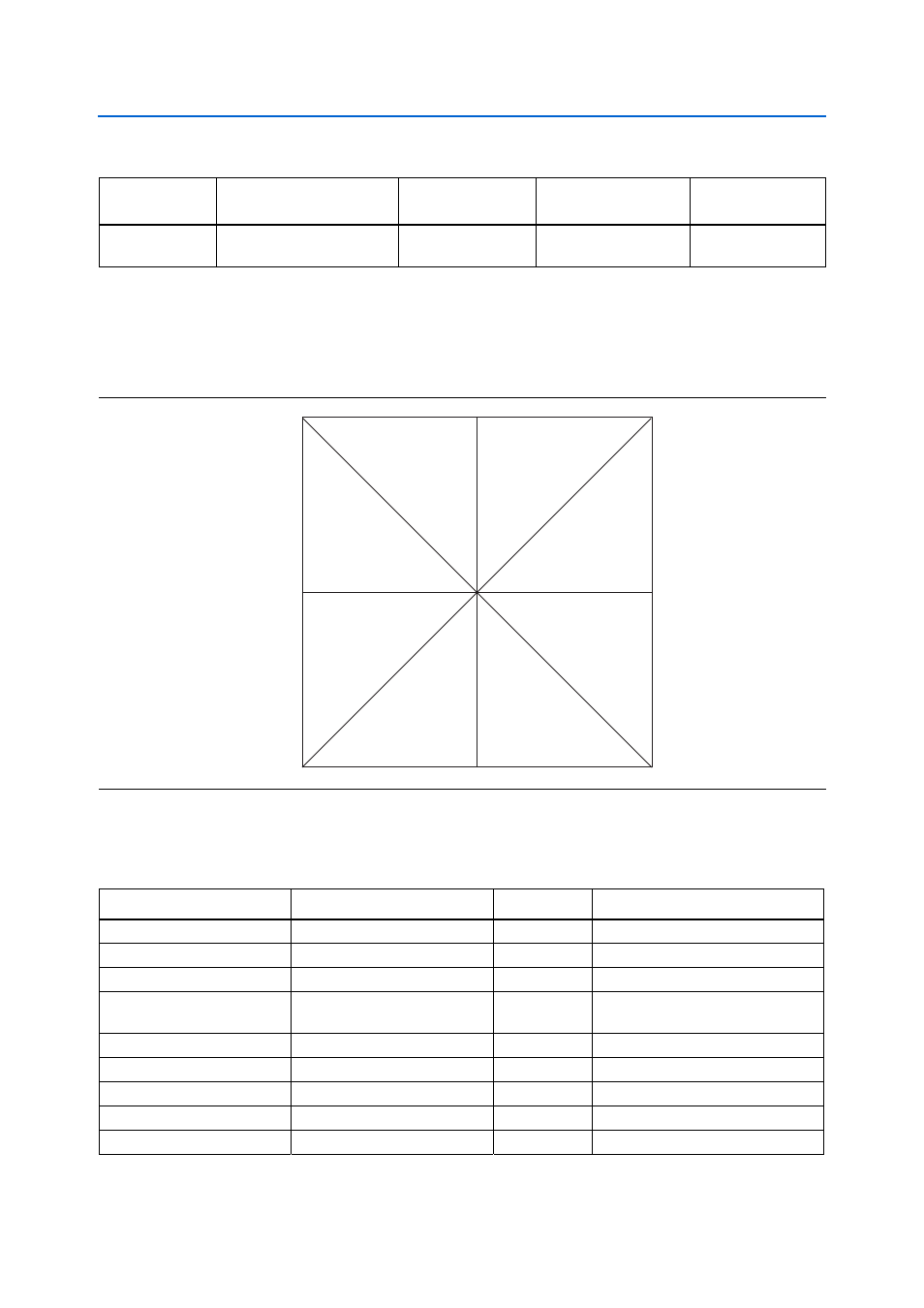
illustrates the bank organization and I/O count for the EP3CLS200 device
in the 780-pin FBGA package.
lists the Cyclone III LS device pin count and usage by function on the
development board.
Table 2–3. Cyclone III LS Device Component Reference and Manufacturing Information
Board Reference
Description
Manufacturer
Manufacturing
Part Number
Manufacturer
Website
U15
FPGA, Cyclone III LS F780,
198K LEs, lead-free
Altera
Corporation
EP3CLS200F780C7N
Figure 2–2. EP3CLS200 Device I/O Bank Diagram
B8
58 I/O
B7
59 I/O
B6
48 I/O
B5
52 I/O
B4
58 I/O
B3
59 I/O
B2
49 I/O
B1
47 I/O
Table 2–4. Cyclone III LS Device Pin Count and Usage (Part 1 of 2)
Function
I/O Standard
I/O Count
Special Pins
DDR2
1.8-V SSTL
94
2 differential clocks, 4 DQS
MAX Bus
2.5-V CMOS
8
—
Flash, SSRAM, FSM Bus
2.5-V CMOS
82
—
HSMC Port A
2.5-V CMOS + LVDS
84
34 LVDS, 2 differential clock inputs, 1
clock input
HSMC Port B
2.5-V CMOS
84
1 differential clock input, 1 clock input
Gigabit Ethernet
2.5-V CMOS
16
1 clock input
Buttons
1.8-V / 2.5-V CMOS
5
1 DEV_CLRn
Switches
1.8-V CMOS
5
—
LCD
2.5-V CMOS
11
—