User-defined leds, User-defined leds –25 lcd –25 – Altera Cyclone III LS FPGA Development Board User Manual
Page 33
Chapter 2: Board Components
2–25
General User Input/Output
© October 2009 Altera Corporation
Cyclone III LS FPGA Development Board Reference Manual
User-Defined LEDs
The development board includes four general purpose LEDs. This section describes
all user-defined LEDs. For information on board-specific or status LEDs, refer to
“Status Elements” on page 2–16
.
Board references D25 through D28 are four user-defined LEDs which allow status and
debugging signals to be driven to the LEDs from the FPGA designs loaded into the
Cyclone III LS device. The LEDs illuminate when a logic 0 is driven, and turns off
when a logic 1 is driven. There is no board-specific function for these LEDs.
lists the user-defined LED schematic signal names and their corresponding
Cyclone III LS pin numbers.
lists the user-defined LED component reference and the manufacturing
information.
LCD
The development board contains a single 14-pin 0.1" pitch dual-row header that
interfaces to a 16 character × 2 line Lumex LCD display. The LCD has a 14-pin
receptacle that mounts directly to the board's 14-pin header, so it can be easily
removed for access to components under the display. You can also use the header for
debugging or other purposes.
The LCD signals are multiplexed with HSMC port B data signals HSMB_D65 through
HSMB_D75
. The LCD/HSMC port B data select header switch (J18) is used to control
data multiplexing on the LCD signals and the HSMB_D[65:75] signals to the
Cyclone III LS device. If the shunt is not placed on the jumper, the FPGA can control
the LCD_HSMB_SEL signal. When the LCD_HSMB_SEL signal is set to '1' (shunt
removed), the FPGA controls the HSMB_D[65:75] signals. When the
LCD_HSMB_SEL
is set to '0' (shunt installed), the FPGA controls the LCD signals. The
default value is set to '1'.
summarizes the LCD pin assignments. The signal names and directions are
relative to the Cyclone III LS FPGA.
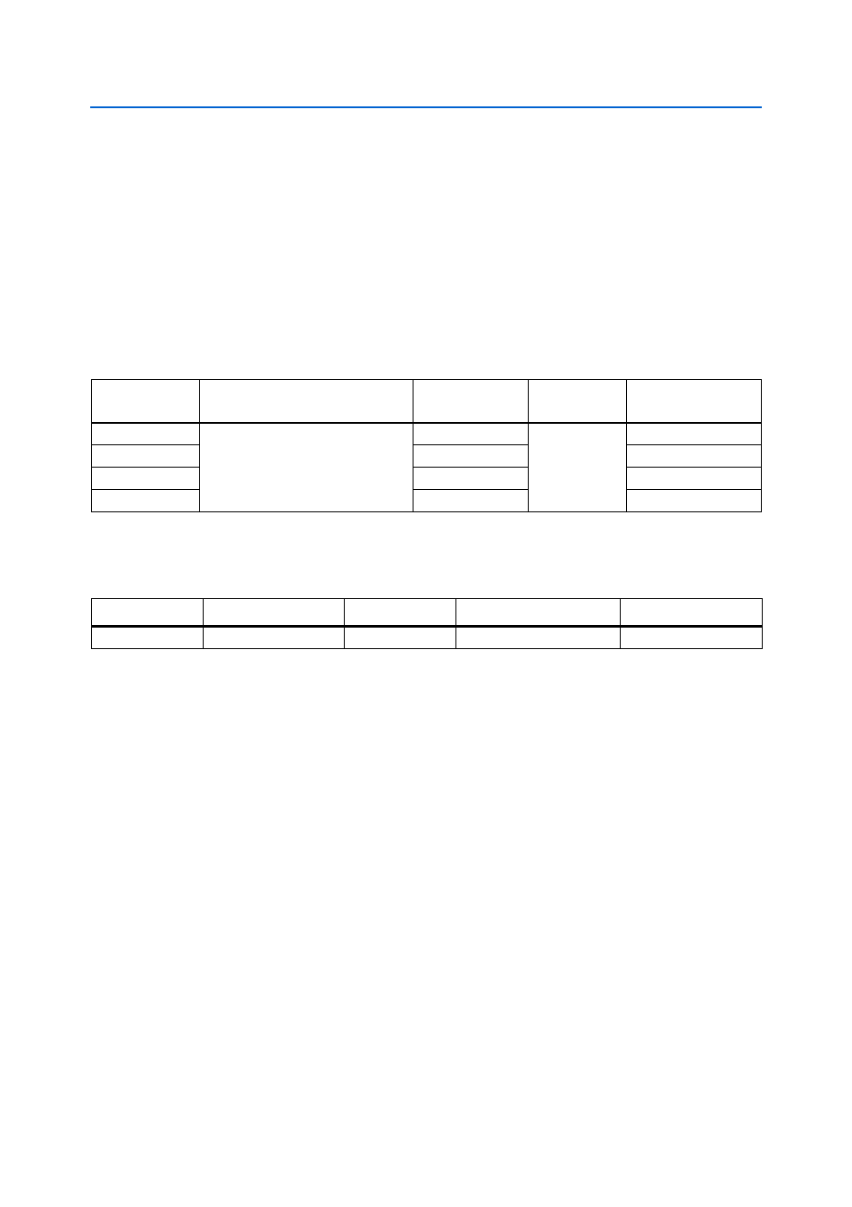
Table 2–27. User-Defined LED Schematic Signal Names and Functions
Board Reference
Description
Schematic
Signal Name
I/O Standard
Cyclone III LS Device
Pin Number
D28
User-defined LEDs.
Driving a logic 0 on the I/O port turns
the LED ON. Driving a logic 1 on the
I/O port turns the LED OFF.
USR_LED0
1.8-V
E24
D27
USR_LED1
G18
D26
USR_LED2
C21
D25
USR_LED3
C7
Table 2–28. User-Defined LED Component Reference and Manufacturing Information
Board Reference
Device Description
Manufacturer
Manufacturer Part Number
Manufacturer Website
D25 to D28
Green LEDs
Lumex, Inc.
SML-LX1206GC-TR