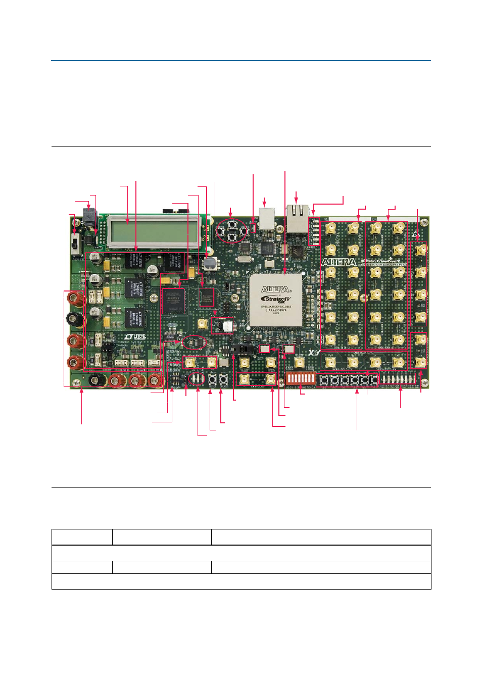
Board overview, Board overview –2, Figure 2–1 – Altera Transceiver Signal Integrity Development Kit, Stratix IV GX Edition User Manual
Page 12: Table 2–1
2–2
Chapter 2: Board Components
Board Overview
Transceiver Signal Integrity Development Kit,
November 2011
Altera Corporation
Stratix IV GX Edition Reference Manual
Board Overview
This section provides an overview of the Stratix IV GX transceiver signal integrity
development board, including an annotated board image and component
descriptions.
shows an overview of the board features.
describes the components and lists their corresponding board references.
Figure 2–1. Overview of the Stratix IV GX Transceiver Signal Integrity Board Features
Note to
(1) The Stratix IV GX Transceiver Signal Integrity board depicted here is the engineering silicon board. For the production silicon board, components
F4, F5, J8, R21, and R23 have been removed and F84 has been added.
Power
Switch
(SW1)
DC Power
Jack (J1)
Power LED (D3)
LCD Display (J24)
Power Circuit (U1-U12)
MAX II CPLD
(U32)
Flash Memory (U39)
Power Select
Switch (SW16)
LCD Directional
Buttons
(SW3-SW6)
Spread Spectrum
Clock (X2, U21)
IO CLK OUT
from FPGA to SMA (J16, J17)
Spread Spectrum
Clock Settings (SW2)
Config
Program
Selection
Jumper
(J62)
User DIP Switches
(SW7)
156.25 MHz Osc (Y5)
External Clock SMA to FPGA
(J14, J15)
100 MHz Osc (Y4)
Socketed
Osc (Y3)
CPU Reset (SW9)
Board Reset (SW8)
Config Status LEDs
(D16-D18)
Fan Connector (J12)
Fan Jumper (J64)
Fan LED (D6)
Embedded
USB-Blaster
Activity LED (D7)
GXB2
TX/RX
SMAs
(J31, J33,
J35, J37)
GXB1
RX SMAs
(J38, J40,
J42, J44,
J46, J48,
J50, J52,
J54, J56,
J58, J60)
GXB1
TX SMAs
(J39, J41,
J43, J45,
J47, J49,
J51, J53,
J55, J57,
J59, J61)
Ethernet
Status
LEDs
(D19-D24)
Embedded
USB-Blaster
(CN1)
Stratix IV GX
FPGA (U33)
10/100 /1000
Ethernet (J68)
User
Push-Buttons
(SW10-SW15)
GXB0
External
SMA
Refclk0
to FPGA
(J19, J20)
User
LEDs
(D8-D15)
External Power
Input Banana
Jacks (J2-J5, J7, J9-J10)
GXB0 TX/RX
SMAs
(J30, J32,
J34, J36)
Table 2–1. Stratix IV GX Transceiver Signal Integrity Development Board Components (Part 1 of 4)
Board Reference
Type
Description
Featured Devices
U33
EP4SGX230KF40
Stratix IV GX device in a 1517-pin FBGA package.
Configuration, Status, and Setup Elements