Altera Transceiver Signal Integrity Development Kit, Stratix IV GX Edition User Manual
Page 17
Chapter 2: Board Components
2–7
Featured Device: Stratix IV GX
November 2011
Altera Corporation
Transceiver Signal Integrity Development Kit,
Stratix IV GX Edition Reference Manual
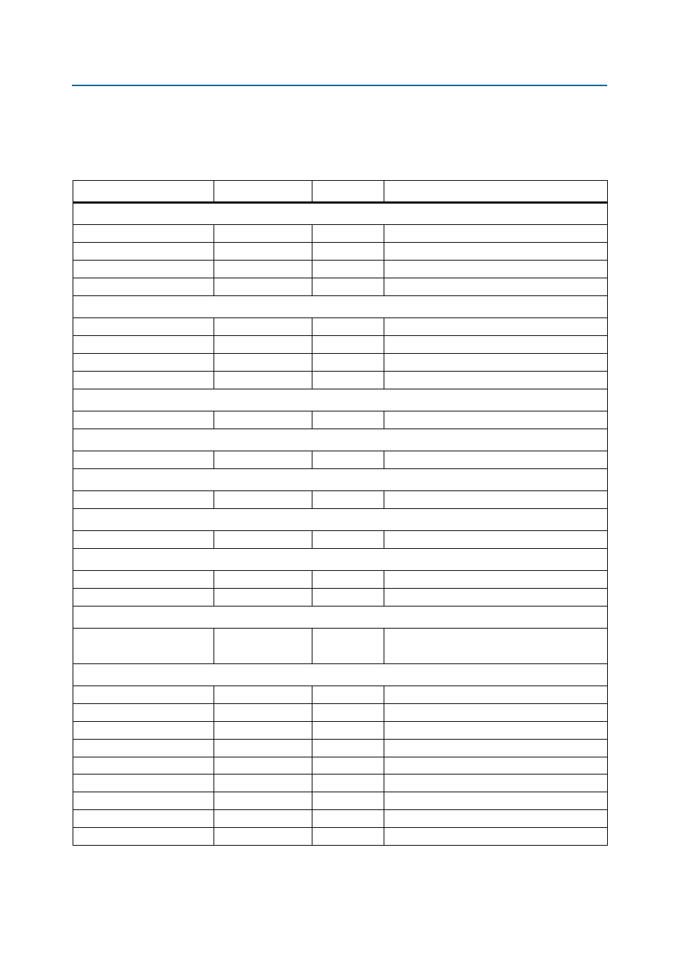
summarizes the FPGA I/O usage by function on the Stratix IV GX
transceiver signal integrity development board. I/O direction is with respect to the
FPGA.
Table 2–4. Stratix IV GX I/O Usage Summary (Part 1 of 3)
Function
I/O Type
I/O Count
Description
FPGA Transceiver Clocks
100-MHz Diff Clock
LVDS input
2
Diff REFCLK Input
Socketed Diff Clock
LVDS input
2
Diff REFCLK Input
156.25-MHz Diff Clock
LVDS input
2
Diff REFCLK Input
SMA Diff Clock Inputs
LVDS input
2
Diff REFCLK Input
FPGA Global Clocks
50-MHz Clock
2.5-V CMOS input
1
Global Clock Input
Spread Spectrum Clock
LVDS input
2
Diff Global Clock
SMA Diff Clock Input
LVDS input
2
Diff Global Clock
SMA Diff I/O or Clock Output
—
2
Diff Global I/O or Clock Output
Temperature Monitor
Temp Sense Diodes
Analog
2
Stratix IV GX Internal Sense Diode
Power Measure
ADC Interface
2.5-V CMOS
5
8 Diff Channel 24-bit A/D Converter
Temp Measure
MAX1619 Interface
2.5V CMOS
4
Die Temp Sense
EEPROM
EEP_CSn
2.5--V CMOS output
1
EEPROM Chip Select
Fan
FAN_On
2.5-V CMOS output
1
Fan Control
FAN_LED
2.5-V CMOS output
1
Fan LED
USB-Blaster
JTAG USB-Blaster or JTAG
header
2.5-V CMOS
4
Built-in USB-Blaster or
JTAG 0.1-mm header for Debug
FPP Configuration
FPGA Dclk
2.5-V CMOS input
1
FPP Dclk
FPGA D[7:0]
2.5-V CMOS input
8
FPP Data
MSEL [2:0]
2.5-V CMOS input
3
Dedicated Configuration Pins
NCONFIG
2.5-V CMOS input
1
Dedicated Configuration Pins
NSTATUS
2.5-V CMOS inout
1
Dedicated Configuration Pins
NCE
2.5-V CMOS input
1
Dedicated Configuration Pins
CONFIG_DONE
2.5-V CMOS inout
1
Dedicated Configuration Pins
INIT_DONE
2.5-V CMOS output
1
Dedicated Configuration Pins
PGM[2:0]
2.5-V CMOS output
3
Configuration Program Select Pins