Dip switch, Flash memory device, Dip switch –18 – Altera Transceiver Signal Integrity Development Kit, Stratix IV GX Edition User Manual
Page 28: Flash memory device –18
2–18
Chapter 2: Board Components
Flash Memory Device
Transceiver Signal Integrity Development Kit,
November 2011
Altera Corporation
Stratix IV GX Edition Reference Manual
DIP Switch
The user DIP switch is for reference design functions and general purpose use. This
switch connects to the FPGA device I/O pins.
summarizes the function
and connections of the user DIP switch (SW7).
Flash Memory Device
The board features a Numonyx PC28F512P30BF 512-Mb CFI-compliant NOR-type
flash memory device. This device stores configuration files for the FPGA. Both the
MAX II CPLD (U32) and FPGA (U33) devices can access the flash. The MAX II CPLD
access the flash for FPP configuration of the FPGA using the PFL Megafunction. The
FPGA access the flash’s user space for embedded NIOS applications.
lists
the pin-out information of the flash memory interface to the FPGA. The signal
direction is with respect to the FPGA device.
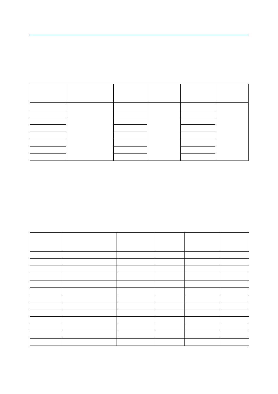
Table 2–15. User DIP Switch Pin-Out (SW7)
Board Reference
Description
Schematic
Signal Name
I/O Standard
Stratix IV GX
Device
Pin Name
Other
Connections
SW7 pin 1
User DIP switch
connected to the FPGA
device. When the switch
is in the open position, a
logic 1 is selected.
When the switch is in the
closed position, a logic 0
is selected.
USR_DIP0
2.5-V CMOS
U33 pin AW27
10-k
Ω pull-up
resistor to 2.5 V
SW7 pin 2
USR_DIP1
U33 pin AU27
SW7 pin 3
USR_DIP2
U33 pin AT27
SW7 pin 4
USR_DIP3
U33 pin AP27
SW7 pin 5
USR_DIP4
U33 pin AN27
SW7 pin 6
USR_DIP5
U33 pin AP26
SW7 pin 7
USR_DIP6
U33 pin AN26
SW7 pin 8
USR_DIP7
U33 pin AM26
Table 2–16. Flash Memory Pin-Out (U39) (Part 1 of 2)
Board
Reference
Description
Schematic
Signal Name
I/O Standard
Stratix IV GX
Device
Pin Name
Other
Connections
U39 pin A1
Flash Address bus bit 1
F_AD1
2.5-V CMOS
U33 pin AN15
U32 pin M16
U39 pin B1
Flash Address bus bit 2
F_AD2
2.5-V CMOS
U33 pin AM14
U32 pin M15
U39 pin C1
Flash Address bus bit 3
F_AD3
2.5-V CMOS
U33 pin AN14
U32 pin M14
U39 pin D1
Flash Address bus bit 4
F_AD4
2.5-V CMOS
U33 pin AP15
U32 pin N16
U39 pin D2
Flash Address bus bit 5
F_AD5
2.5-V CMOS
U33 pin AP14
U32 pin N15
U39 pin A2
Flash Address bus bit 6
F_AD6
2.5-V CMOS
U33 pin AL15
U32 pin J16
U39 pin C2
Flash Address bus bit 7
F_AD7
2.5-V CMOS
U33 pin AP13
U32 pin N13
U39 pin A3
Flash Address bus bit 8
F_AD8
2.5-V CMOS
U33 pin AN13
U32 pin N14
U39 pin B3
Flash Address bus bit 9
F_AD9
2.5-V CMOS
U33 pin J15
U32 pin C14
U39 pin C3
Flash Address bus bit 10
F_AD10
2.5-V CMOS
U33 pin H13
U32 pin B12
U39 pin D3
Flash Address bus bit 11
F_AD11
2.5-V CMOS
U33 pin M13
U32 pin F15
U39 pin C4
Flash Address bus bit 12
F_AD12
2.5-V CMOS
U33 pin M14
U32 pin F16
U39 pin A5
Flash Address bus bit 13
F_AD13
2.5-V CMOS
U33 pin K15
U32 pin D16