Altera Transceiver Signal Integrity Development Kit, Stratix IV GX Edition User Manual
Page 13
Chapter 2: Board Components
2–3
Board Overview
November 2011
Altera Corporation
Transceiver Signal Integrity Development Kit,
Stratix IV GX Edition Reference Manual
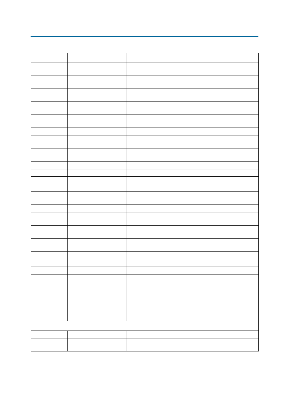
J28
JTAG programming header
JTAG programming header for connecting an Altera USB-Blaster
dongle to program the FPGA and MAX II CPLD devices.
J26
MAX II JTAG configuration
jumper
Jumper to bypass the MAX II CPLD from the JTAG programming
chain.
J63
JTAG for embedded
USB-Blaster MAX II CPLD
JTAG for embedded USB-Blaster MAX II CPLD device programming.
U32
MAX II CPLD
Altera EPM1270256C3N, MAX II 256-pin CPLD for MAX II+Flash FPP
configuration.
D6
Fan LED
Indicates an FPGA over-temperature condition exists and a fan should
be attached to the FPGA and running.
D16–D18
Configuration status LEDs
LEDs to indicate the status of FPP configuration.
J62
Configuration program select
jumper
Jumper to select the flash configuration image to load upon power-on
or reset.
J65
Socketed Y3 OSC
enable/disable jumper
Jumper to enable or disable the Y3 OSC.
J66
Y4 OSC enable/disable jumper
Jumper to enable or disable the Y4 OSC.
J67
Y5 OSC enable/disable jumper
Jumper to enable or disable the Y5 OSC.
D3
Power LED
Blue LED indicates board power status.
D7
USB-Blaster LED
Green activity status LED for embedded USB-Blaster.
D19–D24
Bank of Ethernet LINK and
Status LEDs
Ethernet Link, Speed, Full Duplex, Transmit and Receive activity LEDs.
J6
VCCA voltage selection jumper This jumper selects the V
CCA
voltage to the FPGA.
J11
VCCH voltage selection
jumper
This jumper selects the V
CCH
voltage to the FPGA.
SW16
Power measurement rotary
switch
This switch selects 1 of 6 measured FPGA power rails to display on the
LCD.
SW2
Spread spectrum
configuration DIP switch
DIP switch to set the spread spectrum output clock frequency and
down-spread percentages.
J18
Spread spectrum clock trigger
Spread spectrum clock source routed to SMA for triggering purposes.
J21
Y3 OSC clock trigger
Y3 oscillator clock source routed to SMA for triggering purposes.
J22
Y4 OSC clock trigger
Y4 oscillator clock source routed to SMA for triggering purposes.
J23
Y5 OSC clock trigger
Y5 oscillator clock source routed to SMA for triggering purposes.
J14, J15
Differential SMA clock input to
FPGA core
SMA for receiving a differential external clock input to the FPGA core.
J19, J20
Differential SMA clock input to
FPGA transceiver
SMA for receiving a differential external clock input to the FPGA
transceiver.
J16, J17
Differential SMA clock output
from FPGA core
SMA for sending a differential clock output from the FPGA core.
Clock Circuitry
Y2, U20
50-MHz OSC and clock buffer
50-MHz clock to FPGA and MAX II CPLD.
Y3, U22
Socketed OSC and clock
buffer
5×7-mm oscillator socket for installing alternate oscillator frequencies
to the FPGA transceivers.
Table 2–1. Stratix IV GX Transceiver Signal Integrity Development Board Components (Part 2 of 4)
(1)
Board Reference
Type
Description