Altera Transceiver Signal Integrity Development Kit, Stratix IV GX Edition User Manual
Page 23
Chapter 2: Board Components
2–13
Configuration, Status, and Setup Elements
November 2011
Altera Corporation
Transceiver Signal Integrity Development Kit,
Stratix IV GX Edition Reference Manual
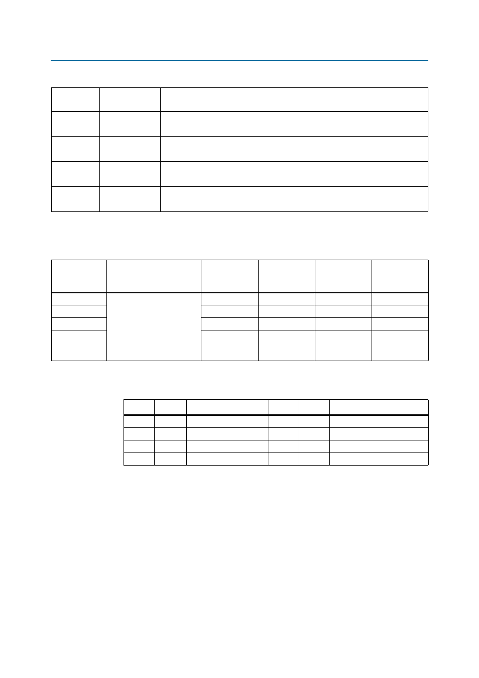
There is a mini-DIP switch (SW2) for configuring the spread spectrum clock device
(U21).
lists the connection of the mini-DIP switch (SW2).
summarizes the mini-DIP switch (SW2) functionality.
J64
FAN
When a jumper is installed on pins 1-2, the fan is automatically controlled by the FPGA.
When a jumper is installed on pins 2-3, the fan is always on.
J65
Y3 OSC
EN/DIS
When a jumper is installed, Y3 oscillator is disabled.
When a jumper is removed, Y3 oscillator is enabled and running.
J66
Y4 OSC
EN/DIS
When a jumper is installed, Y4 oscillator is disabled.
When a jumper is removed, Y4 oscillator is enabled and running.
J67
Y5 OSC
EN/DIS
When a jumper is installed, Y5 oscillator is disabled.
When a jumper is removed, Y5 oscillator is enabled and running.
Table 2–7. Board Jumpers (Part 2 of 2)
Board
Reference
Jumper Name
Description
Table 2–8. Mini-DIP Switch Pin-Out (SW2)
Board
Reference
Description
Schematic
Signal Name
I/O Standard
Stratix IV GX
Device
Pin Name
Other
Connections
SW2 pin 1 (S0)
Spread spectrum clock
configuration DIP switch.
When the switch is in the
open position, a logic 1 is
selected. When the switch is
in the closed position, a logic
0 is selected.
S0
2.5-V CMOS
—
U21 pin 1
SW2 pin 2 (S1)
S1
2.5-V CMOS
—
U21 pin 2
SW2 pin 3 (S2)
SS0
2.5-V CMOS
—
U21 pin 3
SW2 pin 4 (S3)
SS1
2.5-V CMOS
—
U21 pin 8
Table 2–9. Mini-DIP Switch Configuration (SW2)
S1
S0
Clock Frequency
S3
S2
Spread Spectrum %
0
0
25 MHz
0
0
Center ±25
0
1
100 MHz
0
1
Down –0.50
1
0
125 MHz
1
0
Down –0.75
1
1
200 MHz
1
1
No spread spectrum